In a previous article discussing the development process of WiFi chips, we mentioned the FPGA verification of digital circuits.Let’s talk about the development rhythm of WiFi chips.In fact, for any chip with digital circuits, FPGA verification is very important. Although the frequency on an FPGA cannot reach the same level as an ASIC, an FPGA can run the actual software protocol stack, which is still very meaningful for the verification of software and RTL.For the FPGA verification of communication chips, it can be approached from two aspects.
- PHY2PHY Verification
PHY2PHY verification is a purely digital verification method, where two identical DUTs are directly interconnected for transmission and reception verification.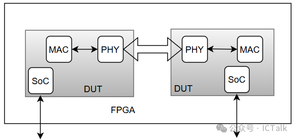 The SoC part is similar to conventional FPGA verification, where various peripheral pins are mapped to the FPGA pins, and then verified through a host computer.For the verification of communication IP, one DUT can be configured as a slave, while the other DUT can be configured as a master for interconnection communication verification. For example, for WiFi, one DUT can be configured as STA, while the other DUT can be configured as AP.This verification method is relatively easy to operate and can verify the entire firmware operation process, but it cannot communicate with actual devices. For instance, in the case of WiFi, it cannot connect to a real AP, which has some limitations.
- MAC+PHY+RF Verification
This verification method only requires one DUT, with the ADC/DAC interfaces of the PHY mapped to the FPGA pins, connected to an external RF board.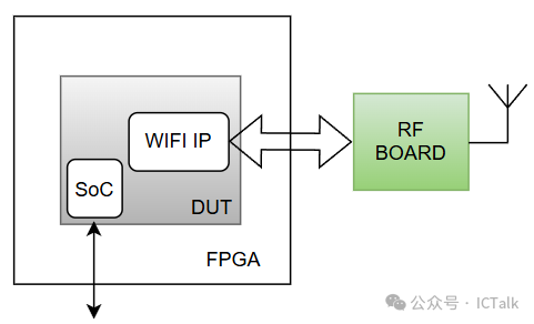 Through the RF card, communication with real AP devices can be established, allowing the entire protocol stack to run and be verified in a relatively realistic scenario.The general analog RF chip used on the RF card is basically the AD9361. The AD9361 provides a 12-bit AD/DA interface, and the FPGA only needs to connect to it according to the timing requirements, and then it can communicate normally through configuration.
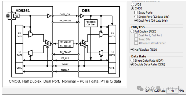 The AD9361 integrates almost all transceiver link modules except for the internal PA. The receiver also supports AGC, and the analog path for transmission and reception integrates multiple stages of filters, which can be programmed and configured according to the bandwidth of different signals.
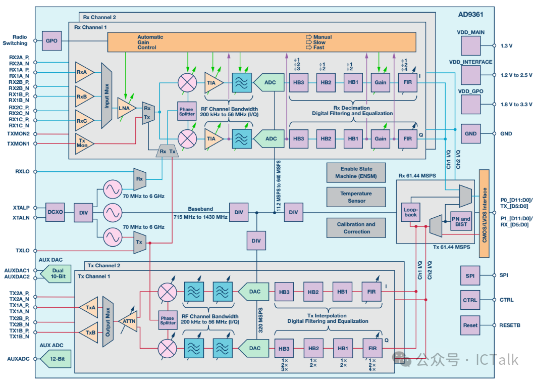 This verification method requires proficiency in using RF boards and the ability to configure them according to one’s needs.In summary, for FPGA verification of communication chips, in addition to purely digital logic verification, external RF cards are usually utilized to better verify communication protocols. Complete FPGA verification can further reduce various bugs in software and RTL design.Done!