The internal memory and I/O port resources of microcontrollers are limited, and in most cases, external expansion is required.
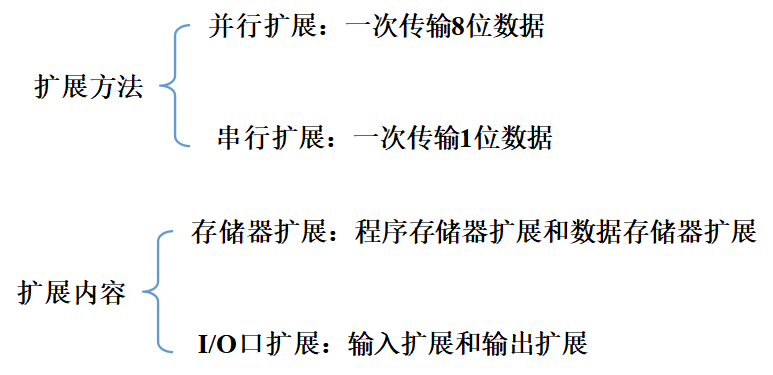
1. Expansion Methods and Content
2. Introduction to Buses
The typical structure for parallel expansion of microcontrollers is a bus structure.
Each expansion component is connected to the microcontroller via the bus, which is equivalent to each component in the system being connected to the bus and utilizing the bus to communicate with the CPU in a time-sharing manner.
When a specific component is selected, it can be read from, written to, and controlled, while other components are in a “high-impedance state” with respect to the bus, effectively disconnected from it.
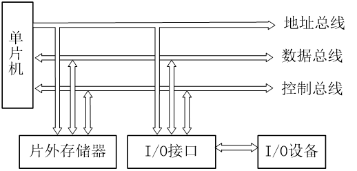
The three-bus structure method for microcontroller systems is as follows:
Using the P0 port lines as the data bus/low address bus and the P2 port lines as the high address bus;
Using function pins to form the control bus.
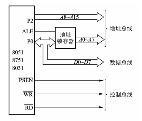
Using the P0 port lines as the data bus/low address bus: First, the P0 port lines serve as the address bus, sending the low 8 bits of the address to the latch, which provides it to the system; then the P0 port lines serve as the data bus to read and write data, thus achieving the sharing of the low 8-bit address signal and data bus on the P0 port without conflict.
Using the P2 port lines as the high address bus: The P2 port lines can provide up to 8 bits of high address, combined with the low 8 bits provided by the P0 port lines, allowing for a maximum of 16 bits of address, enabling the microcontroller system’s addressing range to reach up to 64KB.
Using function pins to form the control bus: The RD (P3.6 pin) and WR (P3.7 pin) serve as read/write selection signal lines; ALE serves as the address latch signal line to cooperate with the P0 port for time-division multiplexing; PSEN serves as the external program memory read selection signal line; EA serves as the selection signal for internal and external program memory.
The basic operation control of memory includes chip selection control and read/write operation control.
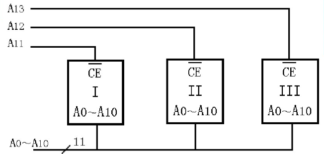
Line Selection Method: The low address lines (A0~A10) achieve internal addressing, while the high address lines (A11~A13) achieve chip selection. The line selection method has simple wiring but results in non-continuous address space, suitable for cases with smaller expansion capacity and fewer chips.
Decoding Method: The high address lines are converted into chip selection signals through a decoder. The decoding method effectively utilizes storage space and provides continuous addresses, suitable for expansion under multiple chips. Commonly used decoder chips include 74138, etc.
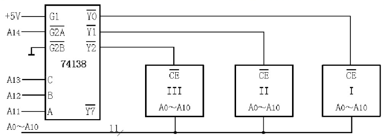
3. Storage Expansion
Address Lines: The address is provided by the P0 and P2 ports. In the ROM address lines (A0~A15), the low 8 bits A0~A7 are connected to the P0 port through the latch 74LS373, while the high 8 bits A8~A11 are directly connected to the P2 port’s P2.0~P2.7.
Data Lines: The 8-bit data line of the external ROM is directly connected to the P0 port of the microcontroller.
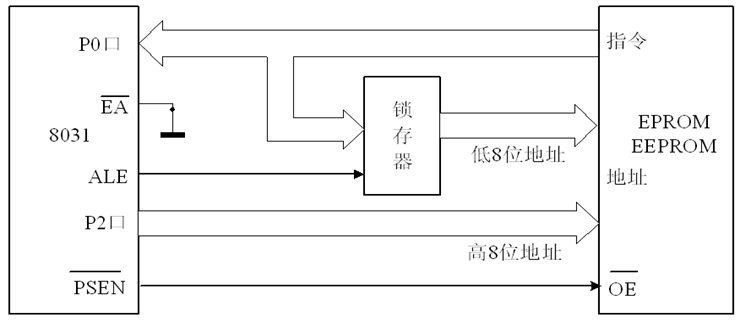
Control Lines: When the CPU executes program instructions stored in the ROM, the instruction fetch phase involves reading from the ROM. The control lines for the read operation include the following:
Address latch signal ALE, chip selection signal CS, read selection signal OE, and external program memory selection control signal EA.
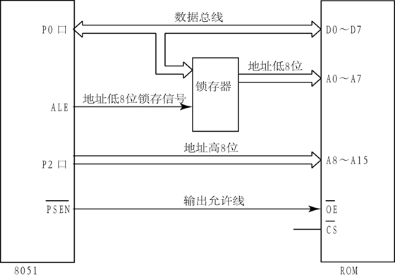
Address Latch Signal ALE: The ALE pin of the microcontroller is connected to the latch’s enable pin G, used to provide the latch signal for the low 8-bit address from the external ROM during instruction reading.
Chip Selection Signal CS: Active low. If only one program memory chip is expanded in the system, the chip selection pin can be directly grounded, keeping the chip always active. If multiple chips are expanded simultaneously, chip selection must be completed using the line selection method or decoding method.
Read Selection Signal OE: Active low. This pin connects to the external ROM read selection signal pin PSEN of the 8051. When accessing the external program memory, as long as a negative pulse appears on this pin, instructions or data can be read from the ROM.
External Program Memory Selection Control Signal EA: When the EA pin is at a high level, the CPU only accesses the internal program memory of the microcontroller and executes instructions from the internal program memory. However, when the program storage exceeds the maximum capacity of the internal program memory, it will automatically switch to execute the program from the external program memory. When the input signal pin is at a low level (grounded), the CPU only accesses the external program memory and executes instructions from the external program memory.
The automatic operation timing of the microcontroller during the execution of external ROM read instructions is as follows:
(1) First, the P0 and P2 ports provide a 16-bit address, then the ALE signal goes low to notify the latch to latch the low 8-bit address from the P0 port;
(2) The PSEN signal goes low, activating the external ROM;
(3) Based on the address provided by the latch and the P2 port, the instruction is fetched and sent to the P0 port, which is then read into the microcontroller for execution.
During this process, the data memory RAM read/write signal terminals WR and RD remain high, isolating the RAM from the bus.
4. Control Program
Write a program based on the circuit in the figure to display the numbers 0-9 in a loop on the digital tube.
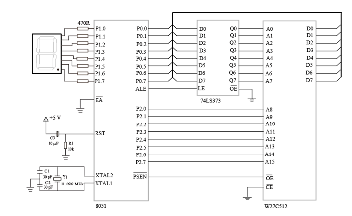
#include <reg51.h>unsigned char led[]={0xC0,0xF9,0xA4,0xB0,0x99,0x92,0x82,0xF8,0x80,0x90};//Character code
int main(void){    unsigned char i;    while(1)  {      for(i=0;i<10;i++)//Loop to display 10 numbers          {               P1=led[i];                   delay();//Delay for a period of time                 }  }}
void delay()//Delay function{     int i,j;      for(i=0;i<3000;i++)    for(j=0;j<5;j++);}
5. Data Storage Expansion
The expansion of data memory RAM mainly utilizes the following three control signals:
ALE: The low 8-bit address latch control signal, usually connected to the LE pin of the address latch;
WR: The external RAM write signal, active low, connected to the WE pin of the data memory;
RD: The external RAM read signal, active low, connected to the OE pin of the data memory.
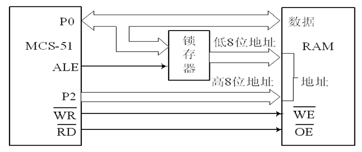
When executing external RAM read/write instructions, the automatic operation timing of the microcontroller is similar to that of reading ROM:
(1) First, the P0 and P2 ports provide a 16-bit address, then the ALE signal goes low to latch the low 8-bit address from the P0 port;
(2) During data reading, the RD signal goes low, and the WR signal goes high, activating the external RAM for reading data based on the address provided by the latch and the P2 port, which is then sent to the P0 port and read into the microcontroller.
(3) When writing data, the data is first loaded into the P0 port, then the RD pin goes high, and the WR pin goes low, activating the external RAM for writing, and the data from the P0 port is written to the external RAM based on the address provided by the latch and the P2 port.
6. Program Example
Write a program based on Figure 8-4 to store the character codes for displaying the numbers 0-9 in the 6264, and then read the character codes from the 6264 in a loop and send them to the digital tube for display.
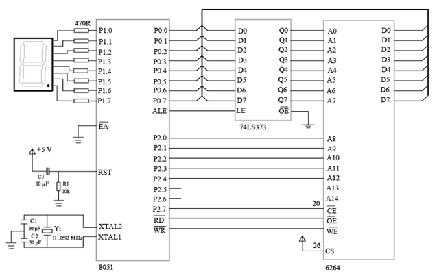
#include <reg51.h>#include  <absacc.h>unsigned char led[]={0xC0,0xF9,0xA4,0xB0,0x99,0x92,0x82,0xF8,0x80,0x90};//Character code
int main(void){    unsigned char i;    for(i=0;i<10;i++)//Store 10 character codes  XBYTE[0x8000+i]=led[i];    while(1)  {      for(i=0;i<10;i++)//Loop to display 10 numbers       {           P1=XBYTE[0x8000+i];           delay();//Delay for a period of time      }  }}
void delay()//Delay function{     int i,j;      for(i=0;i<30000;i++)    for(j=0;j<5;j++);}
For the expansion of input/output port functions, simple TTL circuits or MOS circuits can be used, or more complex programmable interface chips can be utilized.
The MCS-51 microcontroller unifies the I/O ports and external RAM under the same address space, thus using the same 64KB external expansion address space, meaning that the input and output instructions for the I/O ports are also the read/write instructions for the external data memory.
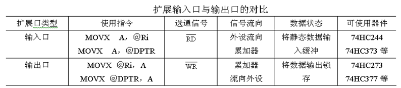
Simple input expansion mainly uses tri-state data buffers to ensure that the selected input device can monopolize the data bus to input data to the microcontroller, while unselected devices are isolated from the data bus. Commonly used tri-state data buffer chips include 74LS244, etc.
Simple output expansion mainly uses tri-state data latches to ensure that the microcontroller can output data to the selected device via the data bus, while unselected devices are isolated from the data bus. Commonly used tri-state data latch chips include 74LS273, etc.
The 8051 microcontroller uses 74LS373 and 74LS245 to expand the I/O ports, connecting to LEDs and DIP switches, requiring the writing of control programs to control the on/off of the LEDs through the toggling of the switches.
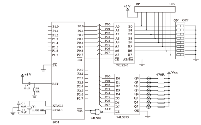
#include <reg51.h>#include  <absacc.h>    #define PORT XBYTE[0xFFFF] //Address can be anything
int main(void){    unsigned char temp;    while(1)    {      temp=PORT; //Read storage unit operation, i.e., get switch data through 74LS245      PORT=temp; //Write storage unit operation, i.e., control LED with switch data through 74LS373    }}
END
Author: JamesBinSource: Embedded Yuxiang GardenCopyright belongs to the original author. If there is any infringement, please contact for deletion.▍Recommended ReadingScary! The CPU hides these undisclosed instructions!How many methods of I2C interface communication do you master?From methods to logic, a super detailed embedded learning roadmap!→ Follow to avoid getting lost ←