
The author of today’s recommended article isChina Electronics Technology Group Corporation No. 58 Research InstituteExpertsZhang Tao, Wan Shuqin, Su Xiaobo, Yu Zongguang.This article is excerpted from the paper “Design of High-Precision DAC Based on High-Speed DDFS“, published in the Journal of China Electronics Technology Research Institute, Volume 10, Issue 6. Let’s start learning together with the editor~
1. Introduction
A digital-to-analog converter (DAC) is a device used to convert multi-bit digital signals into analog signal outputs, serving as an interface between the digital and analog signal domains. High-speed and high-precision DAC devices have become indispensable components in modern electronic systems, widely applied in civilian fields such as wireless base stations, automatic control, medical electronics, video displays, and broadband communications, as well as in national defense and military applications in radar, communications, electronic warfare, and more. In recent years, with the rapid development of digital technology, the demand for high-speed and high-precision DACs has become increasingly urgent. Since the 1970s, China has begun researching DAC technology, and although over a hundred types of DACs have been developed, few have achieved large-scale market applications. Conducting research on high-precision DACs to shorten the technological gap with foreign countries plays a significant role in both national production and defense construction.
This paper introduces a high-speed, high-precision, and high-stability DAC designed based on a 0.13μm process. The circuit has been tested and used in practice, with all technical indicators meeting the expected design goals and stable performance.
2. DAC Structure
The DAC is mainly used to convert digital input signals into analog signals, with inputs typically in parallel binary encoded form and outputs often in current or voltage form. The circuit usually contains a reference voltage source or reference current source, which is converted proportionally to achieve full-scale output. Overall, the function of the DAC device is to quantize the input digital signal into an analog signal.
An ideal DAC can convert N-bit data input codes (DN-1, DN-2……D1, D0) into proportional voltage (or current) outputs, following the relationship: VOUT=KVREFD
where K is the proportional factor, VREF is the reference voltage source, and D is the digital input code.
D=D02-1+D12-2…DN-12-N
where D0 is the most significant bit, and DN-1 is the least significant bit. Combining equations 2-1 and 2-2 gives the output formula for the DAC: VOUT=KVREFD02-1+D12-2…DN-12-N
The equations (1)~(2) indicate that the DAC output comes from the input signal multiplied by the coefficient of the reference voltage, composed of a series of binary weight components. The matching degree between weights is related to the conversion accuracy of the DAC, and achieving higher matching and better output monotonicity is a key design focus for DACs.
The current DAC architectures mainly include voltage-scaled, charge-scaled, and current-scaled types. Among these, the current-scaled architecture performs best. Depending on the encoding method, the current-scaled DAC can be divided into three types: binary-coded architecture, thermometer-coded architecture, and segmented architecture. The binary-coded architecture does not require additional decoding circuits, effectively reducing design complexity, but this structure can lead to oversized high-weight circuits that are difficult to match in high-precision applications. In the thermometer-coded DAC, only one current source turns on or off with each change of 1 LSB, resulting in less jitter in output current and better DNL and INL characteristics; however, the drawback is that for each additional bit of precision, the number of current sources in the array doubles.
To balance speed, accuracy, area, and power consumption, the circuit architecture adopts a segmented structure, as shown in Figure 1. The clock management module provides a reference clock to the data input buffer and decoding module, where the decoded switch signals control the on/off of the 8+6 segmented current source array. The circuit includes an internal reference source that provides a 1.2V reference voltage, with the final output being current-type output, typically using an external 50 ohm load resistor.

Figure 1 Circuit Structure Diagram
3. Circuit Design
3.1 Decoder Design
The decoder part of this circuit is designed as low 8-bit binary code + high 6-bit thermometer code, where the low 8 bits directly control the current source, and the high 6 bits are decoded into 63-bit code to control the current source. Figure 2 shows a schematic of the 14-bit decoder.
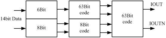
Figure 2 Decoder Schematic
The DAC decoder mainly converts the digital input signal into digital codes used to control the current source switch array to select the required current source transistors. The 14BIT signal adopts a 6+8 two-stage decoding structure, where the high 6 bits use thermometer coding. To suppress the switching timing crosstalk between the switching current sources, a fully differential structure switching current source is adopted, resulting in complementary 63-bit thermometer coding. The low 8-bit signal uses ordinary binary coding to reduce circuit size, yielding a 14-bit binary code. The final output of the decoder is (63+8)×4=284-bit dual zero-pulse code.
The TZ method divides the entire clock cycle into two parts: in the first half-cycle, the output of RTZ is the same as the input, and in the second half-cycle, the output of RTZ returns to zero. The RTZ circuit can reduce code-to-code interference and the SINC roll-off of the D/A converter, lowering the complexity of the reconstruction filter and improving SFDR.However, when outputting large amplitude signals, using the RTZ encoding method causes significant changes in the output signal within half a clock cycle, making it easier for the subsequent driven circuit to enter the linear region and making the DAC output more sensitive to clock jitter, increasing the filtering difficulty for subsequent filters. To overcome the shortcomings of the RTZ encoding method, a dual zero-return coding (DRTZ) method can be adopted, which adds a delayed half-clock cycle waveform of the same RTZ waveform to the original RTZ output waveform, resulting in the final DAC output. Figure 3 shows the simulation waveform of the switch encoding converted to dual zero code under simulation conditions using HSIM5.0, model TT, and a temperature of 25 degrees Celsius, demonstrating that the decoder converts a single switch signal yy<14> into a 4-way zero code signal kk<4:7>.
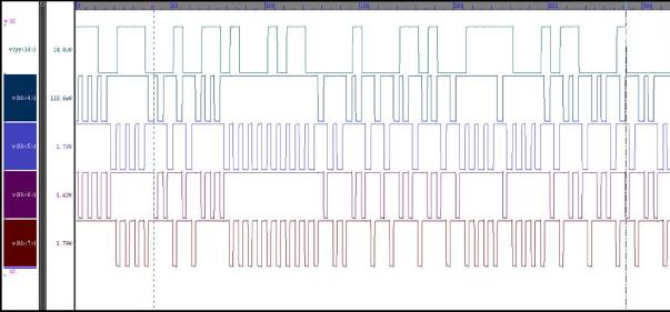
Figure 3 DRTZ Encoding Waveform Diagram
3.2 Current Source and Array Design
The current source unit array is one of the key units in the current steering DAC system. The current matching of the current source unit significantly affects the INL and DNL of the DAC, and transmission nonlinearity can reduce the system’s SNR and SFDR.
The design of the current source array is critical in the current steering DAC circuit design. As analyzed in Chapter 2, system mismatches caused by the process can severely impact the linearity metrics of the DAC and indirectly affect dynamic metrics. Currently, various schemes can optimize matching errors, such as row-column switching schemes, hierarchical switching schemes, dynamic matching techniques, and calibration techniques. In this circuit design, the current source array is arranged based on the Q2 rotational roaming method, consisting of a total of 8*16=128 small arrays, distributing 63 groups of MSB current sources sequentially to positions 2-64 of each small array, while position 1 of each small array is used for the layout of current sources B0~B7. The final layout of the current source array is shown in Figure 4:
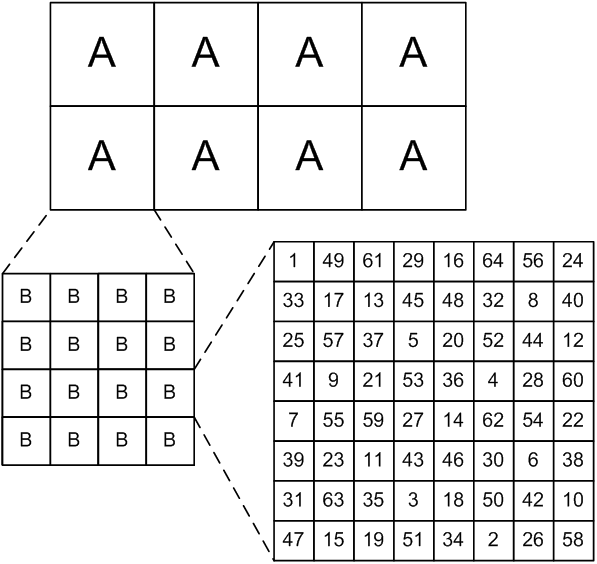
Figure 4 Current Source Array Layout
4. Test Results
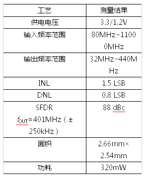
The circuit design considers comprehensive factors such as performance, cost, power consumption, and yield, using a mature 0.13μm CMOS process provided by SMIC with one layer of polysilicon and six layers of metal. The overall chip area is 2.66×2.54mm2, with a working voltage of 1.2V and 3.3V dual power supply.
Figure 5 shows the overall layout of the chip, where the distribution and size of each sub-module can be seen. Figure 6 shows the SFDR test results under a system frequency of 1GHz and an output frequency of 401MHz, with narrowband SFDR approximately 88dBc and broadband SFDR approximately 67dBc. Figures 7 and 8 show the differential nonlinearity error DNL, which is less than 0.8LSB, and the integral nonlinearity error INL, which is less than 1.5LSB.
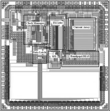
Figure 5 Overall Chip Layout
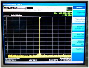
Figure 6 SFDR Test Chart(a) Narrowband SFDR
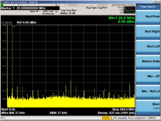
Figure 6 SFDR Test Chart(b) Broadband SFDR
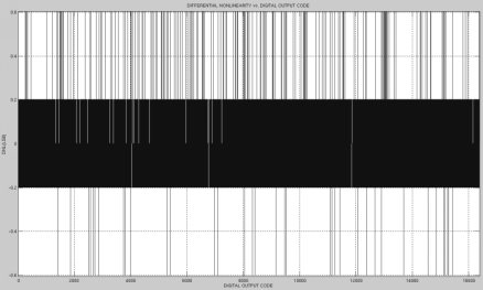
Figure 7 DNL Test Results
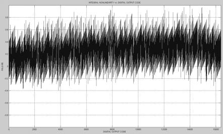
Figure 8 INL Test Results
Table 1 shows the performance parameter indicators of the overall DDS circuit.
Table 1 Main Performance Parameters Measured Values
Conclusion
Based on the SMIC 0.13μm 1P6M mixed-signal CMOS process, a 14-bit, 1GHz DAC circuit has been designed. After tape-out verification and testing, under 1.8V/3.3V power supply and normal temperature conditions, the chip can achieve a maximum clock frequency of 1GHz, with narrowband SFDR ≤ 88dBc and broadband SFDR ≤ 67dBc. INL ≥ 1.5LSB, DNL ≤ 0.8LSB.
(References omitted)
Source: Information and Electronic Frontier
Follow the official account of the China Command and Control Society for exciting content!

【Editor】What military and academic knowledge would you like to know? Feel free to leave a message for us

How to Join the Society
Register as a Society Member:
Individual Members:
Follow the Society’s WeChat: China Command and Control Society (c2_china), reply “Individual Member” to obtain the membership application form, fill it out as required, and if you have any questions, you can leave a message on the public account. You can pay the membership fee online after passing the Society’s review.
Unit Members:
Follow the Society’s WeChat: China Command and Control Society (c2_china), reply “Unit Member” to obtain the membership application form, fill it out as required, and if you have any questions, you can leave a message on the public account. You can pay the membership fee after passing the Society’s review.
Recent Activities of the Society
1. CICC Corporate Member Exchange Meeting
Meeting Time: (Specific time will be notified later)
Long press the QR code below to follow the Society’s WeChat

Thank you for following