Click the blue textto follow us It is well known that for Silicon Carbide MOSFETs (SiC MOSFETs), high-quality substrates can be purchased externally, and high-quality epitaxial wafers can also be obtained from external sources. However, this only provides a good foundation for obtaining a Silicon Carbide device. High-performance Silicon Carbide devices have extremely high requirements for device design and manufacturing processes.
Die Layout
The following image shows a wafer of SiC MOSFET that has completed testing.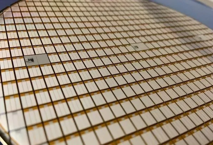
Figure 1
The surface of the chip is generally composed of a Source pad, Gate Pad, and Kelvin Source Pad, as shown in Figure 2. Some chips only have a Gate pad, as the chip in the above image does not have a Kelvin source pad.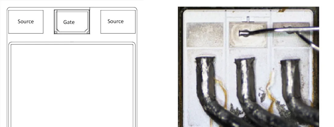
Figure 2
Here we carefully observe that there is a very narrow annular region around the chip, which some call the edge termination ring. This is a vivid description. Its main function is to enhance the chip’s voltage withstand capability, referred to as the Edge termination Ring, usually in a JTE structure. Essentially, a chip is mainly composed of three parts: the Terminal Ring, Gate Pad, Kelvin Source Pad, and the Active Cell. The outer ring of the chip is the edge termination ring, the Gate pad transmits the gate signal to each Cell, and inside are millions of Active Cells. Typically, more attention is paid to the Active Cell, as the switching and conduction performance of the chip is largely related to the Active Cell. Here we summarize the layout of the chip and the characteristics of each part to facilitate a better understanding of the chip.
Edge Termination Ring
-
Surrounds the switching unit of the chip, with most currently adopting a JTE structure.
-
Effectively controls leakage current, improving the reliability and stability of SiC devices;
-
Reduces electric field concentration effects, increasing the breakdown voltage of SiC devices. The breakdown voltage of SiC MOSFETs is related to each switching unit and is also significantly influenced by the edge termination ring.
-
Prevents ionic migration. JTE technology can be used to suppress the drift of mobile ions, thereby enhancing the reliability and stability of SiC MOSFETs. Specifically, JTE technology can form some deeply doped control regions in the edge area of SiC MOSFETs, which can effectively suppress the drift of mobile ions. Additionally, JTE technology can introduce special substances, such as nitrogen and boron, into the control regions, which can chemically react with mobile ions, thus reducing their accumulation and drift in the MOSFET.
Gate Pad and Kelvin Source Pad
-
The Gate pad primarily serves to transmit the gate signal to each switching unit. It is worth mentioning that ON Semiconductor’s chips integrate gate resistors, which can save space and costs in module packaging.
-
The Kelvin Source Pad mainly increases switching speed and reduces switching losses. However, special designs are required when used in parallel.
Active Cell
-
Path for current conduction and cutoff
-
All switching units are in parallel
-
Under fixed unit characteristics, the number of units determines the overall chip’s conduction resistance and short-circuit current capability.
-
Currently mainly divided into planar and trench structures
We have gained an understanding of the surface layout of SiC MOSFETs. In SiC chips, the Edge terminal and Active Cell are two very important parts. ON Semiconductor has rich experience in JTE design, having developed from M1 to M3 in SiC MOSFETs through several generations of technological iterations. The JTE design simulation and manufacturing processes are very mature. Let’s summarize some characteristics and design considerations of JTE.
SiC JTE (Junction Termination Extension) is a structure used to improve the voltage blocking capability of Silicon Carbide (SiC) power devices. The design of SiC JTE is crucial for achieving the required breakdown voltage and avoiding premature breakdown due to high electric fields at the device edges. Here are some key considerations for SiC JTE design:
-
The width and doping of the JTE region: The width and doping concentration of the JTE region determine the electric field distribution at the device edges. A wider and heavily doped JTE region can reduce the electric field and increase the breakdown voltage.
-
The cone angle and depth of the JTE: The cone angle and depth of the JTE affect the electric field distribution and breakdown voltage. A smaller cone angle and deeper JTE can reduce the electric field and increase the breakdown voltage.
-
Surface passivation: The surface passivation layer is crucial for reducing surface leakage and improving breakdown voltage. The passivation layer for SiC JTE devices needs to be carefully designed and optimized.
-
Thermal design: SiC JTE devices can operate at higher temperatures than their silicon counterparts. However, high temperatures may also reduce device performance and reliability. Therefore, thermal design, such as heat dissipation and thermal stress, should be considered during SiC JTE design. Overall, SiC JTE design is a complex process that involves trade-offs between various design parameters. Careful optimization and simulation are required to achieve the desired device performance and reliability.
Active Cell – The Core of SiC MOSFET
The switching unit is a very important part of SiC MOSFETs. We can categorize MOSFETs (Silicon and Silicon Carbide) based on their gate structures into two types: planar structure and trench structure. Their schematic diagrams are shown in Figure 3. From a structural perspective, silicon and silicon carbide MOSFETs are similar, but due to the characteristics of silicon carbide materials and silicon materials, the considerations in manufacturing processes and designs are mostly different. For example, SiC extensively uses dry etching and high-temperature ion implantation processes, and the implanted elements also differ.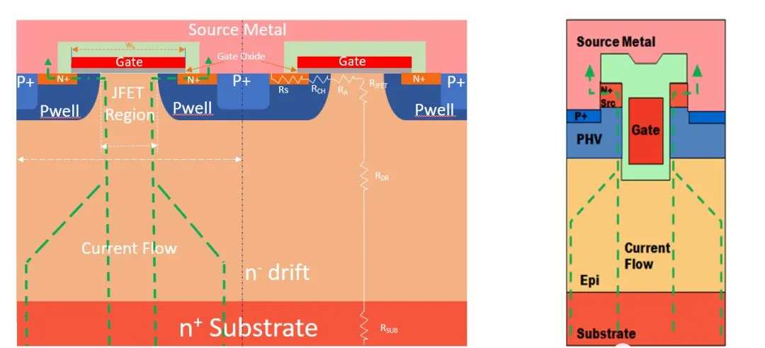
Figure 3
Currently, the vast majority of SiC MOSFETs internationally adopt the planar structure shown in Figure 3A, while a small number of manufacturers use the trench structure shown in Figure 3B. From a developmental perspective, the trend will eventually lead to trench structures. However, the potential of the current planar structure can still be further explored, and trench structures have not yet demonstrated their expected performance. Here we introduce a unified metric to measure their performance – Rsp (Rdson * area), which indicates the conduction resistance per unit area. The planar structure SiC MOSFETs have advantages of high reliability and simple design and processing.The design and manufacturing direction of the Active Cell in planar structure SiC MOSFETs mainly focuses on reducing the pitch value between switching units, increasing the density of switching units, reducing Rdson, and enhancing the reliability of the gate oxide layer.As shown in the structure of Figure 3A, to minimize conduction resistance, adjustments need to be made to the spacing of the switching units, where the pitch value is related to Wg, the width of the gate. As the pitch value decreases, Wg also decreases, which is beneficial for the reliability of the gate. In SiC MOSFETs, the gate oxide layer (Gate Oxide) is very thin, less than 100 nanometers, thus dry etching methods are used in the SiC production process to control processing precision.According to the conduction resistance schematic in Figure 3A, we can derive Rdson=Rs+Rch+Ra+Rjfet+Rdrif+Rsub, where Rch and Ra account for the largest proportion, exceeding 60%, making them a key focus for design and process optimization. However, simply reducing the width of the gate of the switching unit does not necessarily reduce Rsp. If the width of the gate (Wg) is reduced to a certain extent, it may instead lead to an increase in Rsp. Therefore, it is necessary to comprehensively consider the interactions between the above parameters to achieve a more ideal optimization result. ON Semiconductor has developed its planar structure SiC MOSFETs through several generations of process iterations, achieving relative maturity in performance, yield, and reliability.In the chip, each active cell is connected in parallel. Figure 4 is a schematic cross-section of a chip, where a strip structure layout is used. This provides a more intuitive understanding of the chip.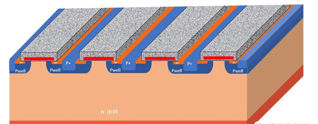
Figure 4: Cross-section of the chip
Below are some key considerations for the design of Rdson in SiC MOSFETs:
-
The channel width and doping: The channel width and doping concentration of SiC MOSFETs affect Rdson and current density. A wider and heavily doped channel can reduce Rdson and improve current carrying capacity.
-
The thickness of the gate oxide layer: The thickness of the gate oxide layer affects gate capacitance, which in turn affects switching speed and Rdson. A thinner gate oxide can improve switching speed but may also increase gate leakage current and the risk of oxide breakdown failure.
-
Gate design: Gate design affects gate resistance, which in turn affects switching speed and Rdson. A lower gate resistance can improve switching speed but may also increase gate capacitance. Overall, the design of Rdson in SiC MOSFETs is a complex process that involves considering the interactions between various parameters. Careful optimization, simulation, and testing are required to achieve the desired device performance and reliability.
Integrated Gate Resistor on Chip
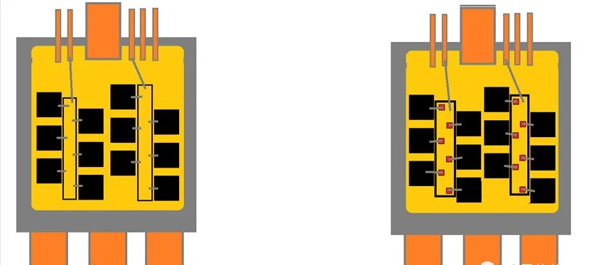
Figure 5
The integrated gate resistor brings several benefits to module design and manufacturing:
-
Simplifies the process of bonding wires in the module, reducing failure rates.
-
Reduces the process of welding resistance to DBC.
-
Decreases BOM and manufacturing costs.
-
Facilitates relatively compact design and manufacturing of packaging.

Wuxi Qixin Semiconductor Technology Co., Ltd. is a high-tech enterprise specializing in the research, development, production, and sales of intelligent production equipment for the chip industry. Established in 2020, it is located in the Wuxi Huishan Economic and Technological Development Zone. The company has received multiple honors, including Wuxi Huishan District Pioneer Talent and Wuxi Taihu Talent, and is a council member of the Wuxi Semiconductor Association. The core members of the company’s R&D team have over 20 years of experience in semiconductor equipment, possessing rich R&D experience in packaging processes and related equipment industrialization, with multiple national-level technology invention, utility model patents, and software copyrights. The company has long-term industry-university-research cooperation with well-known domestic institutions such as Tsinghua University and the Chinese Academy of Sciences.
The self-developed MGP intelligent chip packaging system, AM fully automatic chip packaging system, and TF unit modular chip automatic cutting and forming systems have all received market recognition and unanimous praise from customers.
Wuxi Qixin Semiconductor Technology Co., Ltd. adheres to the values of innovation, efficiency, quality, and integrity, based in Wuxi, with the mission of creating China’s independent brand of intelligent chip equipment, supporting the chip industry, and building smart factories. It aims to become a leader in the chip packaging and testing equipment industry!

Disclaimer: This article is a network reprint or adaptation, and the copyright belongs to the original author. However, due to numerous reprints, it is impossible to confirm the true original author, hence the source is indicated. If there are any copyright issues, please contact us for deletion! The content of this article reflects the original author’s views and does not represent the views of this public account or its responsibility for authenticity.