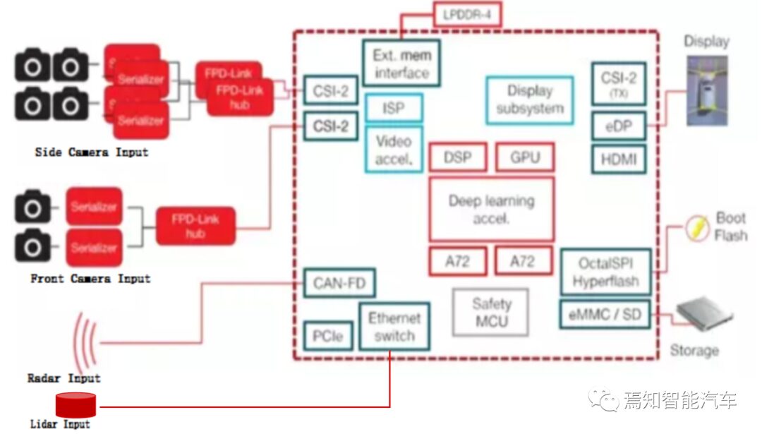
Communication and Storage Technologies for Advanced Autonomous Driving Systems

Advanced autonomous vehicles require high-bandwidth and low-latency networks to connect all sensors, cameras, diagnostic tools, communication systems, and central artificial intelligence. These technologies generate, send, receive, store, and process vast amounts of data.
For the next generation of autonomous driving domain controllers, commonly used in-vehicle networks include CAN, LIN, FlexRay, MOST, and LVDS. Except for LVDS, the others are communication networks specifically designed for the automotive industry. Currently, most vehicles are connected via CAN or LIN, but as data transmission speeds and volumes increase, these buses become less suitable due to their lower bandwidth and larger size. CAN/LIN buses will still have a place, but they will not become the backbone of the communication system.

Communication and Storage Technologies for Advanced Autonomous Driving Systems

The above image shows a centralized domain controller’s internal general connection form. For the next generation of autonomous driving system communication network connections, it mainly involves chip connections in the central domain controller unit, sensor interface input connections, debugging interface connections, storage connections, etc.
Communication and Storage Technologies for Advanced Autonomous Driving Systems
In the central domain controller, it is usually necessary to design a certain size of storage unit for accessing data, programs, files, images, and other information. The designed storage units include Flash, EMMC, LDDR, etc. Among them, Flash generally stores driver program files, with sizes ranging from 32MB to 64MB, while EMMC is primarily used for storing high-precision map data, crowdsourced mapping, autonomous driving data recording, shadow mode, big data, etc., with a size requirement of approximately 96GB to 128GB. LDDR is mainly used for program operation caching. Here, we need to explain several typical forms of communication link hardware, including SPI, UART, GPIO, PCIe, CanFD, FlexRay, and Ethernet.
To illustrate the applicable scenarios for various communication link connection forms, we need to analyze these communication links and their corresponding storage units to varying degrees, explaining their functions, advantages, and disadvantages, focusing on providing assistance and reference for the hardware design of the autonomous driving system domain controller and network communication design process.
Peripheral Communication Buses of System Architecture
The peripheral communication buses of the autonomous driving system mainly refer to the peripheral sensors, storage disks, display units, and vehicle actuators connected to the central domain controller. The data types transmitted by these peripheral sensors and actuator units mainly include raw video data, LiDAR point cloud data, millimeter-wave radar target data, and control/display commands. The main communication connection methods include Ethernet, CanFD/FlexRay/LIN, etc.
The table below shows all typical network connections, storage, and interface information exchange data units in the advanced autonomous driving central domain controller unit, excluding the AI computing unit SOC and logic computing unit MCU.
Communication and Storage Technologies for Advanced Autonomous Driving Systems

1. Ethernet

Why use Ethernet? Simply put, the overall automotive architecture will strongly influence the network direction. Ethernet can reduce the wiring harness while significantly improving service quality in the vehicle network of domain control units. Currently, the architecture of autonomous driving systems is gradually evolving towards a centralized architecture, which means that classic zonal architectures can bring all data distributed across zones into a central location for processing. However, one of the challenges of centralization is bandwidth, which can easily increase to 10Gbps, while the current speed of our vehicular Ethernet is only 1Gbps.
Generally, in peripheral sensor connections, millimeter-wave radar does not require gigabit Ethernet; low-speed Ethernet is sufficient. Cameras can use either Ethernet or traditional LVDS for data communication, but if LiDAR is added, the combination of camera and LiDAR data will require high-speed Ethernet. It is important to note that in high-speed Ethernet PHY integrated into the domain controller, there may be multiple different channels driving 20-30 feet or even longer wiring harnesses simultaneously. This can lead to a significant increase in heat generation within the SOC of the domain controller, which will greatly raise the packaging cost of the entire domain controller.
2. CANFD/FlexRay/LIN
CanFD is the upgraded version of the previous Can network, which only upgraded the protocol while keeping the physical layer unchanged. It features higher bandwidth and data transmission rates. The main differences between CAN and CanFD are transmission rates, data lengths, frame formats, and ID lengths. Additionally, CANFD has variable rates, with the arbitration bit rate being up to 1Mbps (same as CAN), and the data bit rate being up to 8Mbps. Therefore, in the communication network of the next generation of smart driving vehicles, it mainly serves as a progressive network communication unit for transmitting CAN signal communications with higher bandwidth and larger rate requirements.
LIN is a local area network that is a low-cost, serial communication interface with UART. LIN consists of a master node and slave nodes, connected via a single wire. In the next generation of smart driving vehicles, LIN is mainly used in body control applications where communication bandwidth requirements are relatively low, such as steering wheel buttons, windows, and seats, and can serve as a supplement to CAN communication.
FlexRay is primarily aimed at meeting automotive safety and functionality requirements, providing higher transmission bandwidth and higher reliability. It can fully implement all functions of CAN or LIN but is characterized by higher determinism, fault tolerance, and high speed. It is mainly applied in areas with high error tolerance and time determinism requirements, such as next-generation autonomous driving systems, which typically employ steer-by-wire, brake-by-wire, and drive-by-wire for corresponding longitudinal and lateral control. FlexRay is primarily based on differential signal transmission, consisting of two buses, usually using twisted pairs. FlexRay bus transmits data mainly through time-triggered and event-triggered methods, and when using time-triggered communication, it can maintain transmission synchronization and predictability as much as possible, which is very beneficial for the three major control execution units requiring high-speed steer-by-wire control. However, due to its high cost and complex facilities, FlexRay will not completely replace other major in-vehicle network standards.
Inter-chip Communication Buses in High-Performance Computing Platforms
Smart driving advanced domain controllers need to package multiple CPU cores of SOC/MCU/MPU and related auxiliary circuits onto a single motherboard. This multi-chip domain control unit is referred to as the central domain controller. Of course, multi-core multi-chip domain controllers often contain more auxiliary circuits to address communication and coordination issues between multiple CPU cores. Currently, commonly used auxiliary circuit connection methods include GPIO, SPI, UART, PCIe, I2C.
Communication and Storage Technologies for Advanced Autonomous Driving Systems
1. GPIO
GPIO stands for General-Purpose Input/Output bus, which is a flexible software-controlled digital signal. Each GPIO provides a bit connected to a specific pin. Domain control SOC processors heavily rely on GPIO, and in some cases, ordinary pins can be configured as GPIO. Most chips have at least a few sets of similar GPIO. GPIO drivers can be written generically, making it easy for single-board code to pass these pin configuration data to the driver. In advanced autonomous driving AI chips, GPIO often provides power management, audio/video decoding functions, and will frequently have such pins to compensate for the lack of pins on the SOC chip. Here, it is necessary to design some GPIO expansion chips connected to I2C or SPI serial buses.
It should be noted that if using GPIO to simulate the SPI bus, there must be one output pin (SDO), one input pin (SDI), and another pin depending on the specific device type. If implementing a master-slave device, input and output pins are needed; if only implementing a master device, only the output pin is required; if only implementing a slave device, only the input pin is needed.
2. SPI
SPI is a high-speed, full-duplex, synchronous, serial communication peripheral interface bus, operating in a master-slave mode with 3 to 4 line interfaces, allowing multiple SPI devices to connect with each other.
The SPI bus consists of three signal lines: SCLK (serial clock), SDI (serial data input), and SDO (serial data output). When there are multiple slave devices, a slave selection line can be added to control whether the chip is selected, enabling multiple SPI devices to connect on the same bus, such as connecting multiple Flash devices to a chip. We typically use SPI as the communication connection method for Nor Flash, resolving the hardware compatibility issues when different capacities of Nor flash have different numbers of data and address lines, and also ensuring that different capacities of SPI Nor flash pins are compatible with smaller packaging, occupying appropriate PCB board space. SPI Nor Flash transmits one bit of data at a time, with a simpler interface, slower speed, but high cost-performance ratio. For the central domain controller, Nor flash is mainly used to store user data and basic programs; generally, the real-time requirement for the entire storage process is not high, and serial data methods can usually be used to write data into Nor Flash in advance.
The SPI device providing the serial clock is the SPI master or master device, while other devices are SPI slaves.
3. UART
UART is a universal asynchronous receiver-transmitter bus, characterized by two lines, full-duplex, and asynchronous serial communication, with a more complex structure than SPI and I2C. It generally consists of a baud rate generator (producing a baud rate equal to 16 times the transmission baud rate), a UART receiver, and a UART transmitter, with hardware consisting of two lines, one for sending and one for receiving.
As part of the interface, UART can provide the following functions:
  • UART is used to control the central computing unit and serial devices, providing an RS-232C data terminal device interface, allowing the domain controller chip to communicate with modems or other serial devices using RS-232C interfaces;

  • Parallel/serial conversion: converting parallel data transmitted by SOC into output serial data streams;

  • Serial byte conversion: converting incoming serial data from external CPU units into bytes for use by internal parallel data devices of MCU;

  • Parity check: adding parity bits and start/stop flags to the output serial data stream and performing parity checks on the data streams received from external sources;

  • Input/output buffer, managing data and synchronization issues between the domain controller and external serial devices (such as cameras);

4. PCIe
The PCIe bus uses an end-to-end connection method, where only one chip device can be connected at each end of a PCIe link, and these two chips serve as data senders and receivers. In addition to the bus link, PCIe also adopts a model hierarchy similar to network protocol stacks, where the data being sent and received passes through this hierarchy. In high-performance computing platform design, PCIe is often used to transfer images, point clouds, and other information between different SOCs. The chip processing logic within the domain controller adopts a parallel data processing method. The two most important performance parameters are bandwidth and transmission real-time.
We generally focus on effective bandwidth, but many factors affect the effective bandwidth in PCIe, making it difficult to calculate. Typically, we can only estimate the peak bandwidth of a PCIe link for a rough assessment.
Peak bandwidth = bus frequency × data bit width × 2
The table below shows the relationship between bus data width and peak bandwidth in PCIe. Understanding PCIe peak bandwidth can help us design better hardware selection in the domain controller process, selecting appropriate sizes of PCIe based on overall data, image, and point cloud transmission requirements. The highest version of PCIe, V3.0 specification, uses a bus frequency of 4GHz, which will further improve the peak bandwidth of PCIe links.
Communication and Storage Technologies for Advanced Autonomous Driving Systems
PCIe links use a serial method for data transmission, but within chips, the data bus remains parallel; thus, PCIe link interfaces need to perform serial-parallel conversion, which introduces significant delays. This is also the biggest drawback in the application of PCIe. In addition, the data packets on the PCIe bus must pass through the transaction layer, data link layer, and physical layer, and these data packets will also introduce delays when traversing these layers.
Communication and Storage Technologies for Advanced Autonomous Driving Systems
PCIe Bus Layer Composition Structure
In the domain controller, PCIe links use an end-to-end data transmission method. At both ends of a PCIe link, the SOC/MCU chip ports are completely equivalent, serving as sender and receiver, and only one sending device or receiving device can be connected at one end of a PCIe link. Therefore, PCIe links must use a switch to extend the PCIe link to connect multiple devices.
In the PCIe bus, the switch is akin to a switch device, consisting of one upstream port and multiple downstream ports.
5. I2C
I2C stands for Inter-Integrated Circuit bus, a serial communication bus that uses a multi-master-slave architecture, facilitating effective communication between the central domain controller system and peripheral sensors. Due to its simplicity, it is widely used for communication between microcontrollers MCU/SOC and sensor arrays, EPROMs.
Communication Interfaces in High-Performance Intelligent Driving Platforms
1. MIPI – CSI/DSI
MIPI is a mobile industry processor interface, typically used to adapt to the next generation of autonomous driving systems DSI, CSI (Display Serial Interface, Camera Serial Interface). DSI defines a high-speed serial interface between the processor and display module, which is a lane-scalable interface, with 1 clock lane and 1-4 data lanes. The physical layer definitions for DSI and CSI are provided by D-PHY. In next-generation advanced intelligent driving systems, DSI is typically used to connect and input ultrasonic radar data, while CSI defines a high-speed serial interface for communication between the processor and camera module.
Communication and Storage Technologies for Advanced Autonomous Driving Systems
2. Serializer/Deserializer
In the architecture of advanced intelligent driving systems, peripheral sensor components often trend towards high bandwidth and large data, which may exacerbate wiring difficulties, increase power consumption, and raise packaging costs. Typically, the central domain controller processes serial data; thus, it is necessary to first convert the output signals from sensor video into serial/parallel (add serial) and to convert the input signals to the display unit into parallel/serial (remove serial).
As shown in the image above, FPD-Link is an interface for point-to-point video transmission. This interface utilizes SerDes technology to transmit high-definition digital video and bidirectional control channels over twisted pairs or coaxial cables. This allows for optimization between the domain controller unit and the camera or between the display unit and the camera. Additionally, different sampling clocks ensure the synchronized transmission of video and data streams over the same physical channel.
In the video image processing process, we can refer to this as image serialization, which facilitates network transmission, protocol interpretation, and data storage. Meanwhile, employing serializer/deserializer (SERDES) technology’s high-speed serial interfaces to replace traditional parallel bus architectures can reduce wiring conflicts, lower switch noise, and decrease power consumption and packaging costs.
Conclusion
The processing capability of advanced autonomous driving domain controllers relies not only on providing powerful computing and high-performance image processing chips but also on the internal inter-chip communication networks, storage units, and peripheral bus transmission and interface designs. The communication network design emphasizes bandwidth, rate, stability, and avoidance of communication conflicts. Storage units require storage capacity and stability. Peripheral interfaces focus more on interface adaptability and the degree of connection with the communication network bus. Each of these aspects must be fully considered in the actual PCB design of the domain controller. This article provides designers with certain references for hardware selection in various transmission and storage aspects based on overall analysis. Furthermore, if we delve deeper, it will involve actual resistors, capacitors, and even wiring rules, which will not be elaborated on in this article.
Recommended Reading:

◆EE Architecture | Evolution of Autonomous Driving Functional Architecture

◆Sensor Perception | Analysis of Fusion Solutions from Two Different Perspectives: FOV and BEV

◆Domain Controller | Analysis of Trends in Intelligent Driving Domain Controller Hardware Solutions

◆Sensor Perception | Understanding Feature-Level Fusion in BEV Space in One Article

Leave a Comment