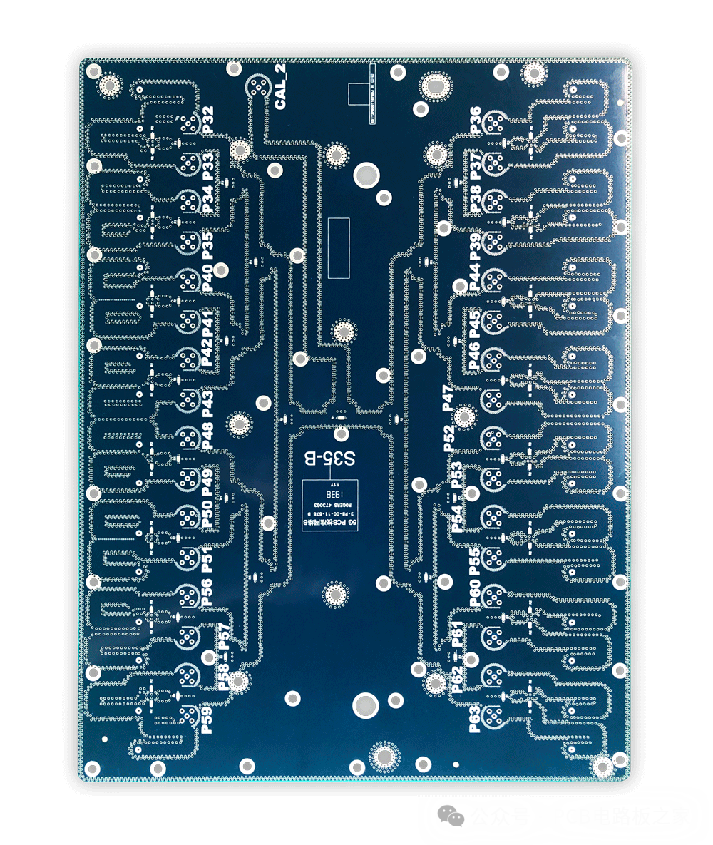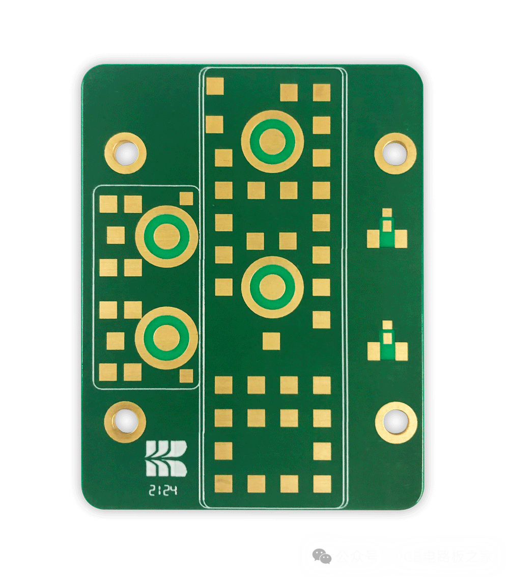
During the PCB prototyping process, various issues may arise that affect the quality of the final product. This article will share some common problems and solutions encountered during PCB prototyping. These issues include design file errors, inaccurate dimensions, and more. By reading this article, users can quickly identify the causes of faults and take appropriate measures to ensure smooth production.

Common Troubleshooting Methods for PCB Prototyping:
1. Design File Errors
Solution: Carefully check and verify the design files before submission. Use professional design software to ensure that the circuit diagrams and layouts comply with electrical specifications and manufacturing requirements. If necessary, conduct additional design reviews or seek third-party assistance.
2. Improper Material Selection
Solution: Choose appropriate PCB materials based on the application environment and performance requirements of the electronic product. If uncertain about material properties, consult experienced suppliers or refer to relevant industry standards for guidance.
3. Soldering Defects
Solution: Ensure the correct soldering techniques and equipment are used. For soldering issues, check the solder, temperature settings, and the skills of the operators. Regular maintenance and calibration of soldering tools are also key to preventing problems.
4. Inaccurate Dimensions
Solution: Verify that the correct PCB dimensions and tolerance settings are used. Communicate with the manufacturer to confirm their production capabilities meet design requirements. Implement strict quality control procedures during production to monitor dimensional accuracy.

5. Electrical Testing Failures
Solution: Conduct comprehensive electrical testing, including insulation resistance testing, continuity testing, and functional testing. Once issues are identified, trace back to potential fault points such as pads, vias, or wiring, and make adjustments or repairs.
6. Surface Treatment Issues
Solution: Select appropriate surface treatment methods and ensure that the parameters during the treatment process are correctly controlled. For issues after surface treatment, it may be necessary to re-clean or re-treat the surface.
7. Signal Interference
Solution: Implement shielding measures, such as shields or shielding layers, to reduce the impact of electromagnetic interference and radio frequency interference. Additionally, arrange ground and power lines reasonably to avoid parallel routing of signal and power lines, minimizing signal interference.
Problems during the PCB prototyping process can usually be resolved through careful design, appropriate material selection, precise manufacturing processes, and strict quality control. When encountering issues, systematically analyzing the causes and taking targeted solutions is key. Maintaining good communication with manufacturers and staying informed about the latest manufacturing technologies and material information can also help avoid potential problems. By employing these methods, issues during the prototyping process can be minimized, ensuring efficient and high-quality PCB production.


Partial Screenshots of Electronic Books

