Remember to star the public account ⭐️ to receive notifications promptly.
 Source:ContentTranslated fromphotonics。
The optical field rooted in classical precision mechanics and the semiconductor industry defined by microelectronics miniaturization, once distinctly different sectors, are increasingly overlapping at the forefront of innovation. This convergence is not coincidental. Rather, it is the result of shared technological challenges and the fusion of manufacturing techniques, partly due to the demands of optical components exceeding the limits of traditional processing methods. To meet these stringent requirements, manufacturers are increasingly adopting technologies originally established for semiconductor manufacturing processes.
The growing number of applications requiring a balance of advantages from both fields is another decisive factor in this thriving overlapping domain. Semiconductor manufacturing is a well-established driver of process standardization, material innovation, and nanometer-level precision. Today, as these capabilities advance into the optical manufacturing frontier, manufacturers are applying them to develop solutions. These solutions range from freeform lenses for space telescopes to nanostructured surfaces in photonic integrated circuits (PICs)—solutions that are increasingly favored as scalable high-performance telecommunications and advanced data processing solutions.
Moreover, adaptive optics and meta-optics are redefining beam control and wavefront shaping, enabling dynamic control of light with unprecedented precision within compact form factors.
The blurring of boundaries between semiconductors and precision optics is also evident in materials and technologies. For instance, silicon carbide (SiC), traditionally used for power electronics and harsh and extreme environment applications, is being explored for high-performance optical devices. This material exhibits good thermal stability and mechanical stability, reflecting the growing cross-fertilization in the field of materials science. Broadly, materials science is expanding through advanced crystals, nonlinear optical materials, and metamaterials. Advances in these areas contribute to enhancing wavelength coverage, optical efficiency, and durability.
At the same time, although precision optics is downstream in the value chain, away from those key technology areas that have proven transformative, manufacturing technologies are driving upward growth in precision optics. Breakthroughs in sub-wavelength lithography, atomic layer deposition, and ultrafast laser processing are directly propelling the development of precision optics and photonics at the forefront of science, industry, and defense. These manufacturing methods enable the production of optical components with nanometer-level precision, powering ultra-sensitive sensors, high-power laser systems, and compact optical components for quantum computing and lidar.
For example, lithography technology, which previously existed solely in the domain of chip manufacturers, has now become a foundational technology for creating sub-wavelength optical structures. Even semiconductor-driven disciplines such as statistical process control, advanced metrology, and chemical mechanical planarization are bringing practicality to optical manufacturing, improving the quality and yield of increasingly complex component geometries.
These cross-industry implementations are not isolated adjustments. They reflect a deeper reintegration of the design, manufacturing, and refinement methods of optics and semiconductors. From shaping the lithographic optical components that define each semiconductor node to polishing materials that transcend wafer fabrication and telescope mirror production, manufacturers are redefining the boundaries between these two industries. As precision, scale, and complexity push both fields to their limits, their shared challenges are giving rise to common solutions.
However, challenges remain, particularly in thermal management, cost-effective mass production, and integration with existing electronic systems. Nevertheless, the trajectory of development in precision optics and photonics is undoubtedly upward.
Precision Polishing: The Art and Science
The surface quality required for advanced optical components is one of the most demanding steps in the manufacturing process. With extremely high requirements for surface accuracy, smoothness, and shape fidelity, it faces a range of complex challenges. Even minute defects at the nanometer level can significantly degrade optical performance, especially in high-power laser systems, space telescopes, and interferometers. Achieving such specifications requires highly controlled environments, advanced metrology techniques, and precision polishing technologies.
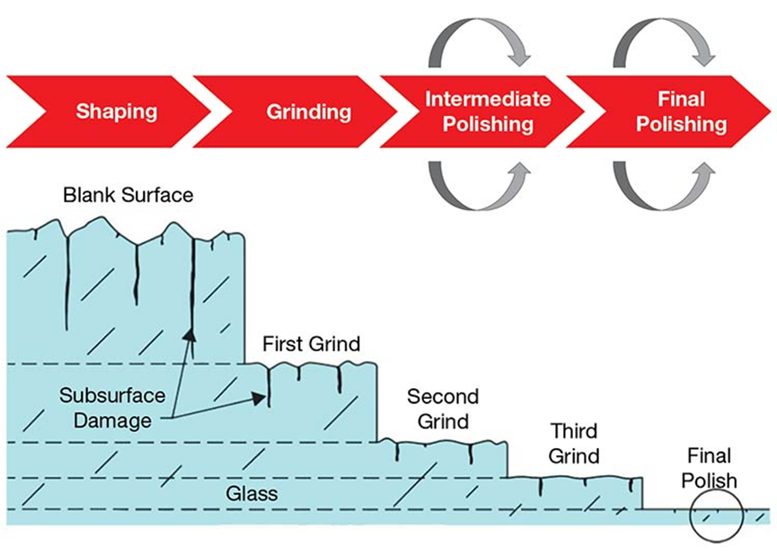
Technologies such as magnetorheological polishing, ion beam processing, and computer-controlled polishing are increasingly becoming standards in production. Additionally, different materials such as fused silica, sapphire, and calcium fluoride respond differently to polishing processes. Avoiding subsurface damage or stress-induced birefringence becomes a challenge, often requiring customized approaches and/or the use of different materials during the production phase.
Defect control, particularly preventing polishing residues and subsurface contamination, is equally important. Minute residues from polishing agents, such as cerium oxide particles, can embed in the surface of optical components and act as absorption points under high-power laser exposure. Such defects can significantly lower the laser-induced damage threshold and potentially lead to catastrophic optical component failure. Multiple studies have shown that polishing slurries and pads can generate carbon or abrasive residues, which may require plasma post-treatment to remove these contaminants and restore the laser-induced damage threshold.
Today, as the geometries and applications of optical components become increasingly complex, maintaining a uniform removal rate, avoiding edge effects, and achieving consistent surface quality are becoming more challenging. The growing prevalence of freeform and aspheric optics exacerbates this challenge. The geometries of these optical components pose particular challenges to traditional polishing methods due to their non-rotationally symmetric profiles, tighter tolerances, and more stringent functional requirements.
Thus, precision polishing is no longer merely an art; it is a science. It requires a deeper understanding of material properties, tool dynamics, and process adaptability than ever before.
In this context, the emergence of mid-spatial frequency errors represents a particularly persistent challenge.
Mid-Spatial Frequency Errors
Mid-spatial frequency errors refer to surface irregularities with spatial wavelengths typically between 0.12 and 5 millimeters, lying between low-frequency shape deviations and high-frequency roughness. Typically, sub-aperture polishing or deterministic finishing processes are the causes of these mid-spatial frequency ripples. During these machining processes, repetitive tool paths or oscillating tool movements can create periodic surface structures. These features may not appear in standard shape measurements but can degrade the performance of optical systems by inducing diffraction, increasing scattering, or lowering the Strehl ratio, particularly in high-resolution imaging or high-power laser applications.
To control these effects, manufacturers are implementing pseudo-random tool paths, incorporating dedicated smoothing steps, and using power spectral density-based metrology techniques to monitor mid-frequency components throughout the polishing and/or finishing process. These strategies are crucial for providing optical components that not only meet overall shape requirements but also satisfy the local surface quality needed for next-generation optical systems.
Coating and Metrology:
Among the various processes initially developed for microelectronics, atomic layer deposition (ALD) has become a standard in the optical industry, now capable of producing optical components with nanometer-level precision and complex geometries. It is widely used in modern optical coatings, capable of depositing conformal, pinhole-free films with atomic-level control over thickness. This method is highly valuable for producing high-performance anti-reflective coatings, interference filters, and durable protective layers on optical components with complex geometries.
Moreover, these coatings exhibit excellent uniformity, environmental durability, and extremely low optical loss—all critical characteristics for advanced photonic applications such as high-power laser optical components and integrated photonic circuits. As a result, optical systems are becoming more compact, efficient, and integrated, opening up new possibilities in fields such as photonic computing, advanced sensing, and high-resolution imaging.
Precision metrology is another area of advancement driven by progress in the semiconductor industry, pushing improvements required for the stringent specifications of advanced optical components, from wafer inspection to optical component quality measurement. Many technologies used in the semiconductor industry are now widely applied to assess the surface roughness, shape accuracy, and material uniformity of optical substrates and coatings. These technologies include interferometry, white light profilometry, scattering measurements, and optical and atomic force microscopy.
These testing and measurement methods provide nanometer to sub-nanometer resolution, enabling manufacturers to detect and correct defects that may affect optical performance. This is crucial in micro-optics manufacturing. As the sizes of optical components continue to shrink and their complexity increases, especially in the fields of PICs and freeform optical components, the demand for high-throughput, non-contact, and automated metrology solutions will surge. By leveraging the speed, accuracy, and scalability of semiconductor inspection technologies, optical manufacturers can maintain stringent tolerances and improve yield, quality, and repeatability throughout the production cycle.
The Era of Enhanced Vision:
The fusion of semiconductor-level metrology, atomic-level coatings, and precision optics is not merely theoretical—it is already transforming the real-world technologies that connect the digital and physical worlds. This is particularly evident in the rapidly evolving fields of augmented reality and mixed reality, where the demand for ultra-compact, high-performance optical systems is directly intertwined with semiconductor innovations. Fundamentally, as display technologies shrink in size and computational power continues to grow, user expectations are also rising. The need for optical devices that meet nanometer-level tolerances while remaining lightweight, durable, and scalable has become critical. Meta’s Orion glasses are a prominent example of this fusion, highlighting how semiconductor-driven precision technologies empower a new generation of wearable optical devices. The Orion augmented reality platform integrates Micro-LED projectors into custom SiC optical components, achieving exceptional miniaturization and optical clarity in an ultra-lightweight form factor. This system combines next-generation display technologies, eye and hand tracking, and AI interfaces—all relying on precision optical engineering that was initially tested and refined in semiconductor manufacturing processes. The Orion prototype also provides clear evidence that sub-millimeter component alignment, advanced coatings, and wafer-level tolerances have transcended the cleanroom domain to become the foundation of consumer device performance. Orion
is still in the prototype stage. Nevertheless, it offers a glimpse into the future: everyday devices will require optical and material precision as advanced as that found in state-of-the-art semiconductor fabs. In the future, the fields of optics and microelectronics will be deeply intertwined, facing shared challenges including miniaturization, thermal management, and system integration.
Interdisciplinary Collaboration for High Performance
Pioneering systems like Meta’s Orion prototype embody the dissolution of boundaries between microelectronics and precision optics. As mentioned, this fusion is also changing the materials and consumables that support advanced manufacturing. In fact, precision tools are not limited to system-level breakthroughs—they are also reflected at the microscopic level, in the shaping, polishing, and refinement of surfaces.
Even advancements in semiconductor consumables, such as polishing pads and slurries, can often create direct value in the precision optics field. For example, DuPont’s IC1000 product is one of the most popular polishing pads for semiconductor device manufacturing. This product achieves consistent planarization while minimizing defect rates and overall planar loss, making it a widely used solution in chemical mechanical planarization processes.
Users in the precision optics industry can apply these excellent characteristics to ultra-precision polishing of spherical and aspherical surfaces.
Of course, the benefits brought by these technological advancements are mutual; precision optical components play a critical role in lithography technology, driving the continued miniaturization of electronic components. Similarly, high-performance optical systems are essential for focusing and guiding deep ultraviolet and extreme ultraviolet light with exceptional precision. These optical components must maintain uniformity and stability under high energy loads while achieving diffraction-limited performance to resolve features smaller than 10 nanometers.
Innovations in materials, coatings, and metrology have been key to enhancing optical performance, enabling chip manufacturers to push the boundaries of Moore’s Law. Now, as semiconductor nodes continue to shrink, the demands on lithographic optical systems will become even more stringent, making precision optics a foundational technology for future electronics manufacturing.
This interdisciplinary innovation extends into the abrasive field. Cerium oxide, which has traditionally been used for dielectric planarization in semiconductors, is currently being redesigned for optical-grade applications, as these applications are critical for surface integrity and cleanliness.
Persistent Challenges and Solutions
In most cases, the shapes and forms required for optical parts are achieved during the production process, necessitating final polishing to improve surface quality and geometry while avoiding distortion of the required optical form. The instruments used in final polishing operations are typically rigid tools on which thin polishing pads (known as petal pads or foils) are applied.
The polishing pad materials used in final polishing operations are often polyurethane-based, imparting a random pore structure to the material during manufacturing. This random pore structure was initially developed to aid slurry delivery to increase material removal rates.
However, inconsistent pore structures limit the performance of pad materials in terms of surface quality and consistency between polished parts. In this case, a highly controlled pore structure is needed to achieve better consistency during the polishing process.
This challenge is just one of many brought about by the convergence of semiconductor and precision optical devices. To meet this demand, some manufacturers have introduced a polyurethane material solution that can generate complex 3D shapes that traditional petal polishing pads cannot achieve, particularly suitable for operations involving large radii. This 3D shape can be used in conjunction with computer numerical control or spindle polishing tools, allowing for multiple refinements, regenerations, or modifications throughout its lifespan.
However, not all changes are immediately apparent. For instance, cerium oxide-based polishing slurries are very common in the polishing of silica glass, which is often used in precision optical devices. The particle size of cerium oxide abrasives is typically around 1 micron, providing excellent surface quality for many applications.
However, as technological advancements and application demands continue to raise the bar for such optical surfaces, improvements in process solutions, including polishing slurries and pads, are needed.
The Era of Shared Precision
The fusion of semiconductor manufacturing and optical manufacturing is no longer theoretical. It has reshaped the design, processing, and polishing of precision components. Initially limited to knowledge transfer between industries, it has evolved into a deeper structural coordination, where materials, metrology, and process control developed for the semiconductor industry are addressing long-standing challenges in the optical field.
This integration is not one industry absorbing another, but a shared pursuit of nanometer precision, consistency, and scalability. As the shapes and functions of optical devices become increasingly complex, and as semiconductors move toward smaller nodes and more integrated systems, the overlap between these two fields will only expand. From advanced polishing pads and cerium oxide slurries to atomic-level coatings and sub-nanometer metrology, the building blocks for next-generation optical devices are increasingly influenced by semiconductor-level thinking.
Reference Link
https://www.photonics.com/Articles/From_Circuits_to_Surfaces_Semiconductor/p5/a71248
*Disclaimer: This article is original by the author. The content reflects the author’s personal views, and Semiconductor Industry Observation reproduces it solely to convey a different perspective, not representing Semiconductor Industry Observation’s endorsement or support of this view. If there are any objections, please contact Semiconductor Industry Observation.
END
This is the 4146th issue shared by “Semiconductor Industry Observation”. Welcome to follow.
Recommended Reading
★A Chip that Changed the World
★U.S. Secretary of Commerce: Huawei’s Chips are Not That Advanced
★“ASML’s New Lithography Machine is Too Expensive!”
★The Quiet Rise of Nvidia’s New Competitors
★Chip Crash, All Blame Trump
★New Solutions Announced to Replace EUV Lithography!
★Semiconductor Equipment Giants, Salaries Soar by 40%
★Foreign Media: The U.S. Will Propose Banning Software and Hardware Made in China for Cars

Star the public account ⭐️ to receive notifications promptly, the small account prevents loss.
Seeking likes

Seeking shares

Seeking recommendations