CCTC® Click the blue text above to follow 
Source: Future Think Tank
Hua Xia Climate 30,000+ fans,Welcome to place commercial advertisements, prices are beautiful
Thank you for your recognition and support!

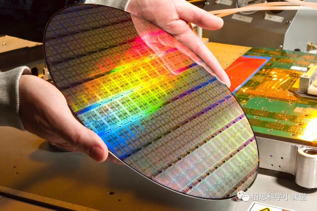
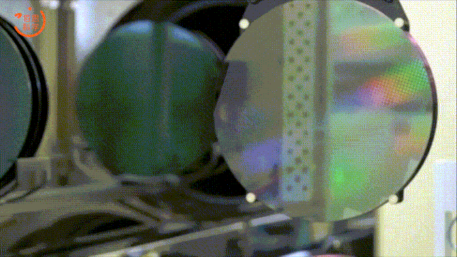
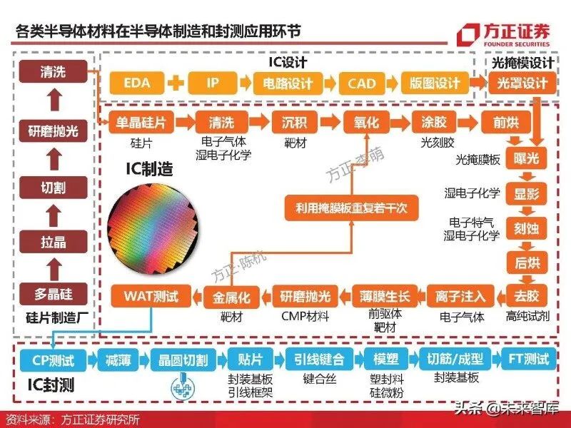
Processed wafers from foundries

Coating photoresist

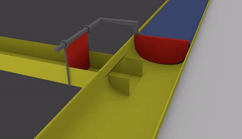
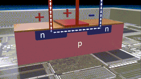
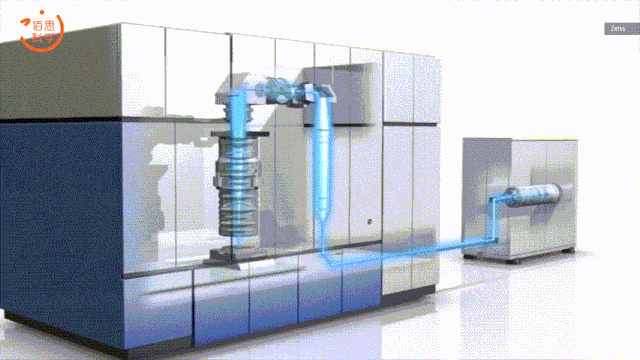
Principle of wafer exposure
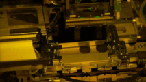
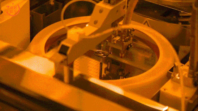
Photo lithography machine for wafer exposure
Internal structure of the lithography machine
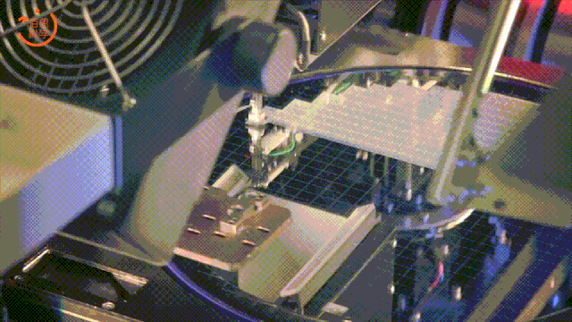
Etching machine in operation

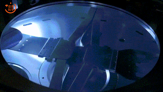
Ion implantation equipment
The following video is from Baishi Science Classroom
Download original text – Leave a message in the background: Eight Major Chip Materials
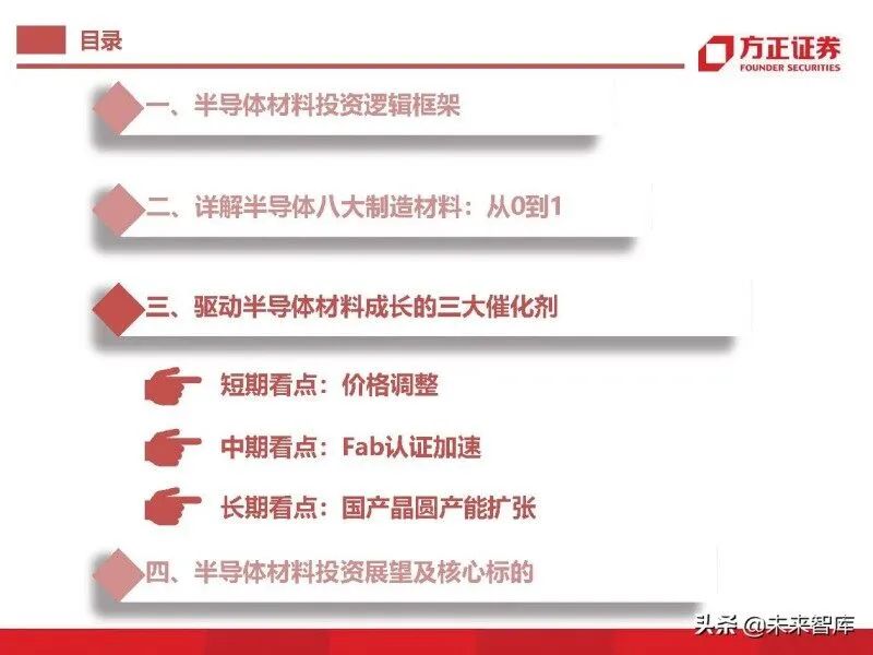
1. In-Depth Explanation of Eight Major Semiconductor Manufacturing Materials: From 0 to 1
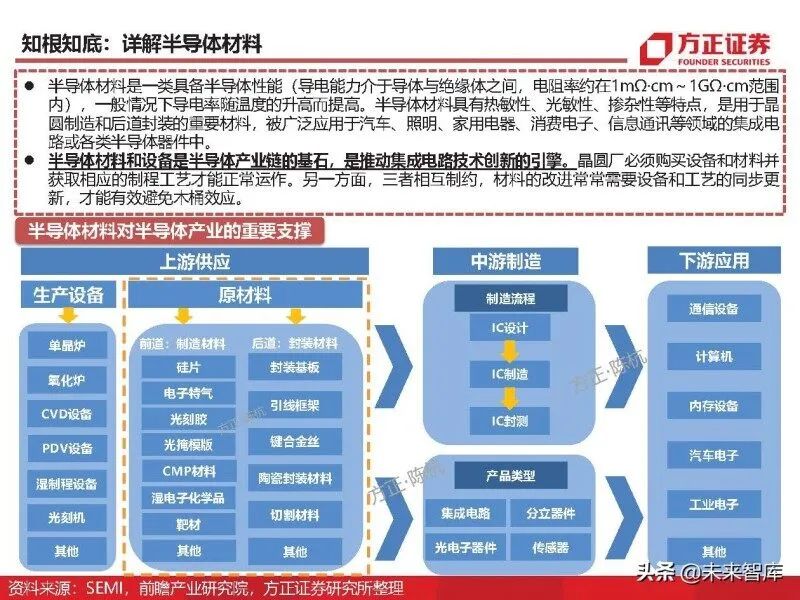
Understanding Semiconductor Materials
Semiconductor materials are a class of materials that possess semiconductor properties (conductivity between that of conductors and insulators, with resistivity typically ranging from 1 mΩ·cm to 1 GΩ·cm). Generally, conductivity increases with temperature. Semiconductor materials exhibit thermal sensitivity, optical sensitivity, and doping characteristics, making them important materials for wafer manufacturing and subsequent packaging, widely used in integrated circuits or various semiconductor devices in fields such as automotive, lighting, home appliances, consumer electronics, and information communication.
Semiconductor materials and equipment are the foundation of the semiconductor industry chain and the engine driving innovation in integrated circuit technology. Wafer fabs must purchase equipment and materials and obtain the corresponding process technology to operate normally. On the other hand, these three are interdependent; improvements in materials often require simultaneous updates in equipment and processes to effectively avoid the “barrel effect”.
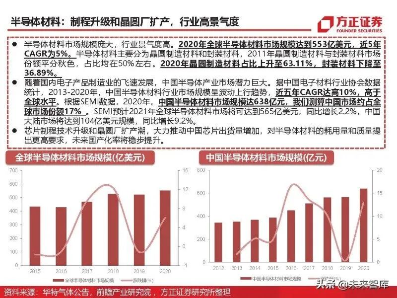
Semiconductor Materials: Process Upgrades and Wafer Fab Expansion, High Industry Prosperity
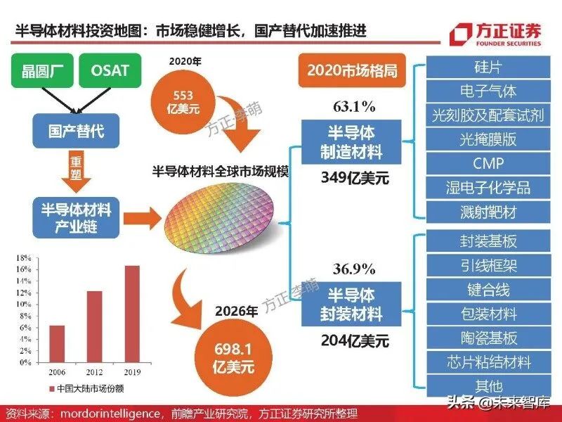
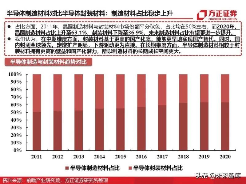
The semiconductor materials market is vast, with high industry prosperity. In 2020, the global semiconductor materials market reached $55.3 billion, with a CAGR of 5% over the past five years. Semiconductor materials are mainly divided into wafer manufacturing materials and packaging materials; in 2011, the market share of wafer manufacturing materials and packaging materials was roughly equal, each accounting for about 50%. By 2020, the share of wafer manufacturing materials rose to 63.11%, while packaging materials decreased to 36.89%.
Comparison of Semiconductor Manufacturing Materials and Packaging Materials: Manufacturing Materials’ Share Steadily Rising
We believe that in the mid-term, packaging materials, due to a higher domestic replacement rate, can achieve domestic substitution earlier. At the same time, domestic testing and packaging are globally leading, and the expansion of fixed assets is evident, with downstream drivers being more direct. In the long term, semiconductor manufacturing materials have higher barriers and domestic potential compared to packaging materials, so the long-term growth space for manufacturing materials is larger.
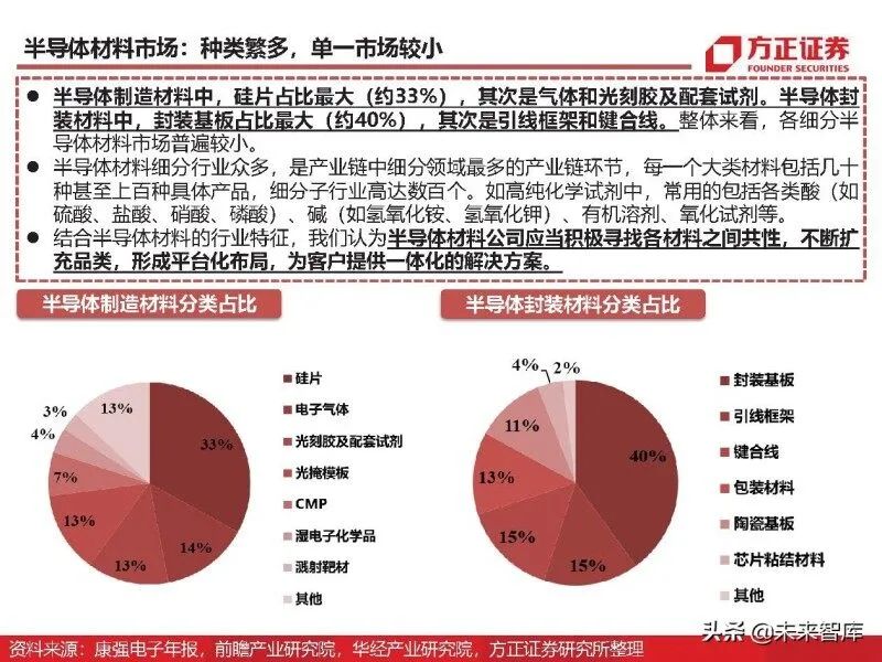
Semiconductor Materials Market: Diverse Types, Small Individual Markets
Among semiconductor manufacturing materials, silicon wafers account for the largest share (about 33%), followed by gases and photoresists and supporting reagents. Among semiconductor packaging materials, packaging substrates account for the largest share (about 40%), followed by lead frames and bonding wires. Overall, the markets for various segmented semiconductor materials are generally small.
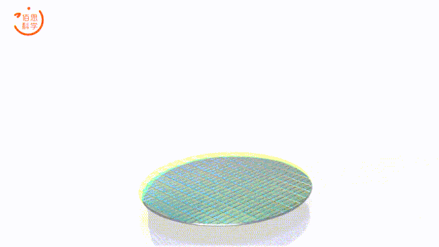
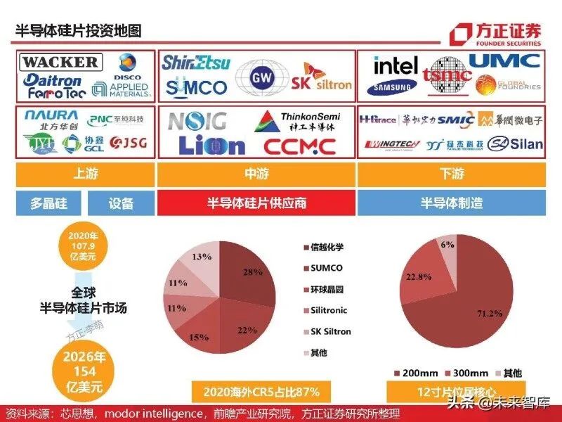
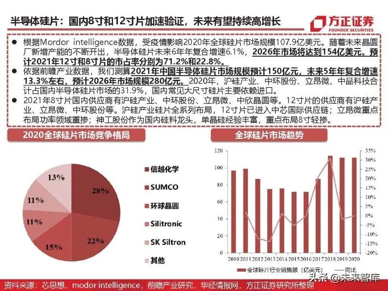
Semiconductor Silicon Wafers: Domestic 8-inch and 12-inch Wafers Accelerate Verification, Expected to Maintain High Growth
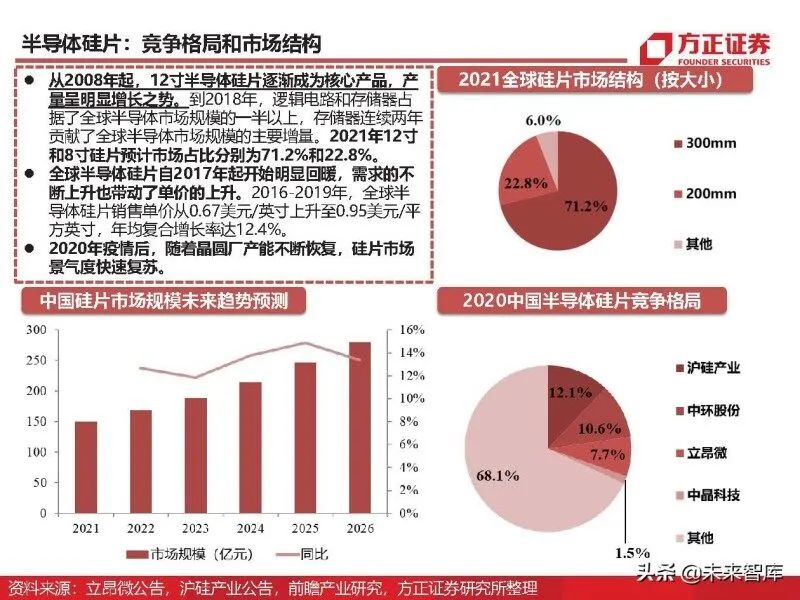
According to Mordor Intelligence data, affected by the pandemic, the global silicon wafer market size was $10.79 billion in 2020. With the continuous opening of new wafer fab capacities in the future, the compound annual growth rate of semiconductor silicon wafers is expected to be 6.1% over the next six years, with the market reaching $15.4 billion by 2026. It is estimated that in 2021, the market shares of 12-inch and 8-inch wafers will be 71.2% and 22.8%, respectively.
Semiconductor Silicon Wafers
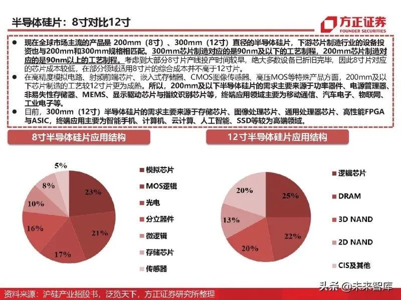
Comparison of 8-inch and 12-inch: Currently, the mainstream products in the global market are 200mm (8-inch) and 300mm (12-inch) diameter semiconductor silicon wafers, and the equipment investment in the downstream chip manufacturing industry matches the 200mm and 300mm specifications. The 300mm chip manufacturing corresponds to process technology of 90nm and below, while the 200mm chip manufacturing corresponds to process technology of above 90nm. Considering that most 8-inch production lines were put into operation earlier, the vast majority of equipment has been fully depreciated; thus, the chip costs corresponding to 8-inch wafers are lower, and in some areas, the comprehensive cost of using 8-inch wafers does not exceed that of 12-inch wafers.
Competitive Landscape and Market Structure: Since 2008, 12-inch semiconductor silicon wafers have gradually become the core product, with a significant growth trend in production. By 2018, logic circuits and memory accounted for more than half of the global semiconductor market size, with memory contributing the main incremental growth to the global semiconductor market for two consecutive years. The market shares of 12-inch and 8-inch wafers in 2021 are expected to be 71.2% and 22.8%, respectively.
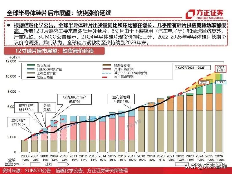
Global Semiconductor Silicon Wafer Market Outlook: Shortages and Price Increases Continue
According to Shin-Etsu Chemical’s announcement, the global shipment of semiconductor silicon wafers is growing both year-on-year and month-on-month, with almost all silicon wafer suppliers operating at high capacity. The new demand for 12-inch wafers mainly comes from logic epitaxial wafers, while 8-inch wafers are in serious shortage due to downstream applications (such as automotive electronics) and global economic recovery. SUMCO’s announcement indicates that the spot price of semiconductor silicon wafers continued to rise in Q4 2021, and the long-term contract price for semiconductor silicon wafers will increase from 2022 to 2026. We believe that the global silicon wafer shortage will last at least until the end of 2023.
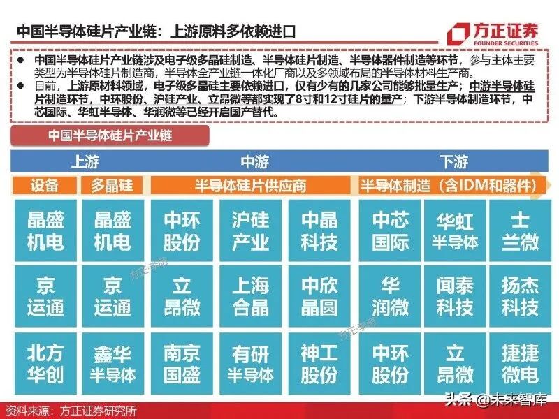
China’s Semiconductor Silicon Wafer Industry Chain: Upstream Raw Materials Largely Depend on Imports
The Chinese semiconductor silicon wafer industry chain involves the manufacturing of electronic-grade polysilicon, semiconductor silicon wafer manufacturing, and semiconductor device manufacturing, with the main participants being semiconductor silicon wafer manufacturers, integrated firms in the entire semiconductor industry chain, and semiconductor material manufacturers with diversified layouts.
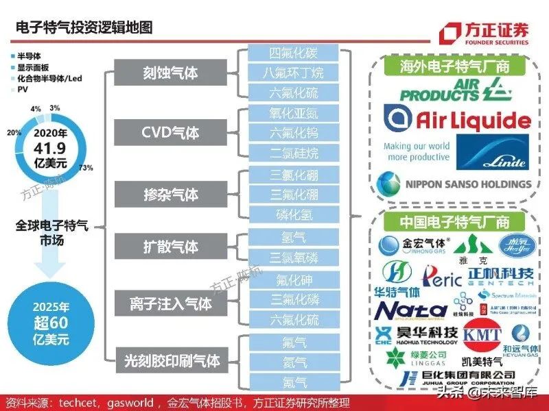
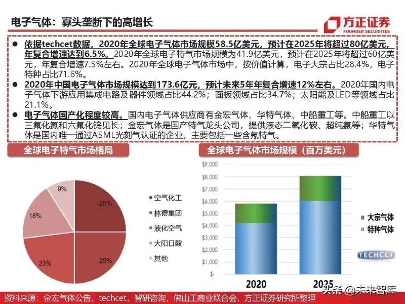
Electronic Gases: High Growth Under Oligopoly
According to Techcet data, the global electronic gas market size was $5.85 billion in 2020, and it is expected to exceed $8 billion by 2025, with a compound annual growth rate of 6.5%. The global market size for electronic specialty gases in 2020 was $4.19 billion, and it is expected to exceed $6 billion by 2025, with a compound annual growth rate of about 7.5%. In 2020, among the global electronic gas market, electronic bulk gases accounted for 28.4% by value, while electronic specialty gases accounted for 71.6%.
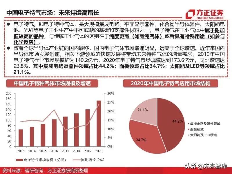
China’s Electronic Specialty Gas Market: Continuous High Growth Expected
Electronic specialty gases are essential support materials in the production of large-scale integrated circuits, flat panel display devices, compound semiconductor devices, solar cells, and optical fibers. Electronic specialty gases are distinguished from traditional industrial gases by their higher purity (such as high-purity gases) or special purposes (such as participating in chemical reactions).
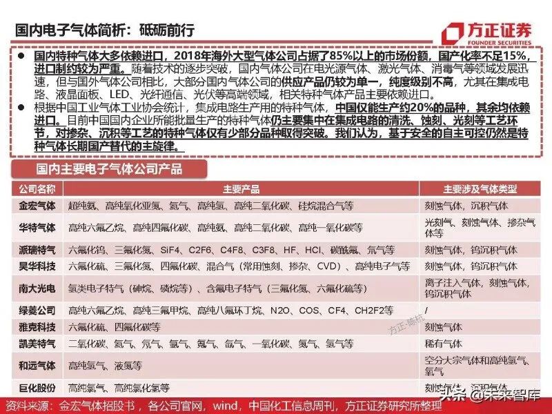
Domestic Electronic Gases Analysis: Progressing Steadily
Most domestic specialty gases rely on imports; in 2018, overseas large gas companies occupied over 85% of the market share, with a domestic replacement rate of less than 15%, and imports are severely constrained. With gradual technological breakthroughs, domestic gas companies have rapidly developed in the fields of light source gases, laser gases, and disinfection gases, but compared to foreign gas companies, most domestic gas companies still offer relatively single product lines with lower purity levels, especially in high-end fields such as integrated circuits, LCD panels, LEDs, optical fiber communication, and photovoltaics, where specialty gas products mainly rely on imports.
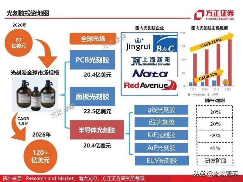
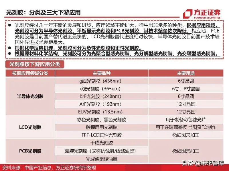
Classification and Three Major Downstream Applications: Photoresists have evolved over decades, expanding their application fields and giving rise to many types. Based on application fields, photoresists can be classified into semiconductor photoresists, flat panel display photoresists, and PCB photoresists, with decreasing technical barriers. Accordingly, PCB photoresists are currently the fastest in domestic substitution, LCD photoresists are relatively fast, and semiconductor photoresists have the largest gap in domestic technology compared to foreign advanced technologies.
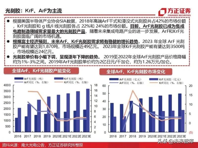
KrF and ArF as Mainstream: According to data from the Semiconductor Industry Association (SIA), in 2018, high-end ArF dry and immersion photoresists accounted for 42% of the market share, while KrF photoresists and g-line/i-line photoresists each accounted for 22% and 24% of the market share. Currently, ArF photoresists have become the most demanded photoresist products in the integrated circuit manufacturing field, and with the further development of the integrated circuit industry, ArF and KrF photoresists face broad market opportunities.
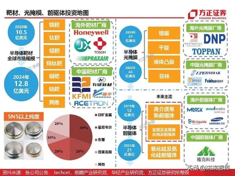
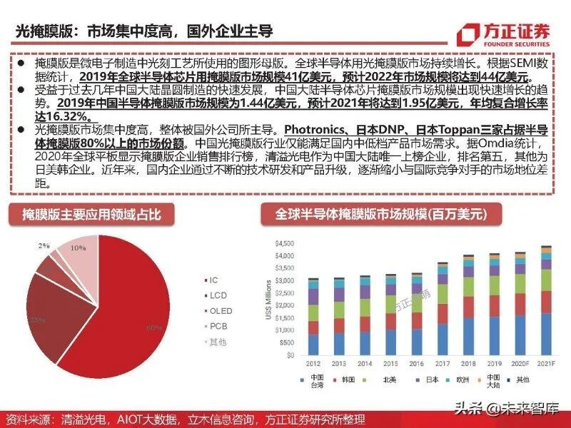
Photo Mask: High Market Concentration, Dominated by Foreign Companies
Photo masks are the pattern templates used in photolithography processes in microelectronics manufacturing. The global semiconductor photo mask market continues to grow. According to SEMI data, the global market size for semiconductor chips using photo masks was $4.1 billion in 2019, and it is expected to reach $4.4 billion by 2022.
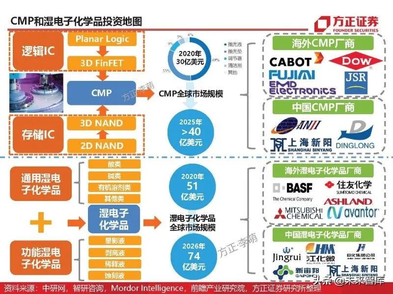
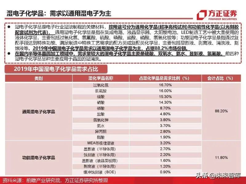
Wet Electronic Chemicals: Demand Mainly for General Wet Electronics
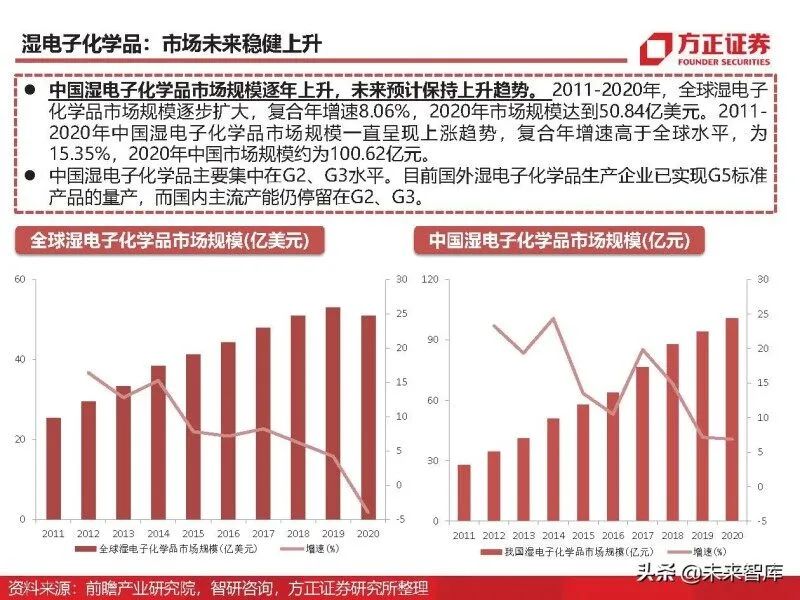
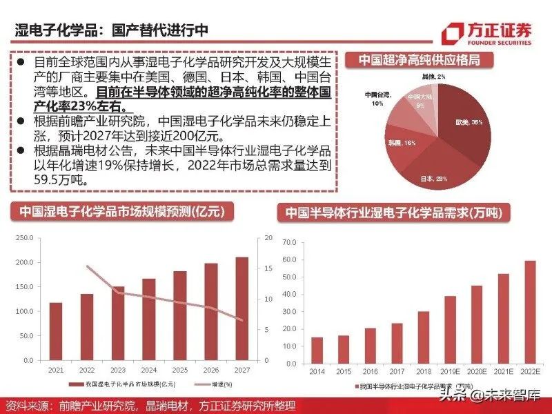
Wet electronic chemicals are key materials for the wet processing in the electronics industry, which can be divided into general chemicals (ultra-pure reagents) and functional chemicals (represented by photoresist supporting reagents). General wet electronic chemicals refer to liquid chemicals widely used in the manufacturing processes of integrated circuits, LCD panels, solar cells, and LEDs, mainly including hydrogen peroxide, hydrofluoric acid, sulfuric acid, phosphoric acid, hydrochloric acid, nitric acid, and ammonium hydroxide; functional wet electronic chemicals refer to formula or compound chemicals that achieve special functions to meet specific process needs in manufacturing, mainly including developers, strippers, cleaning solutions, and etching solutions. In 2019, the demand for wet electronic chemicals in China was mainly for general wet electronic chemicals, accounting for 88.2% of the market share.
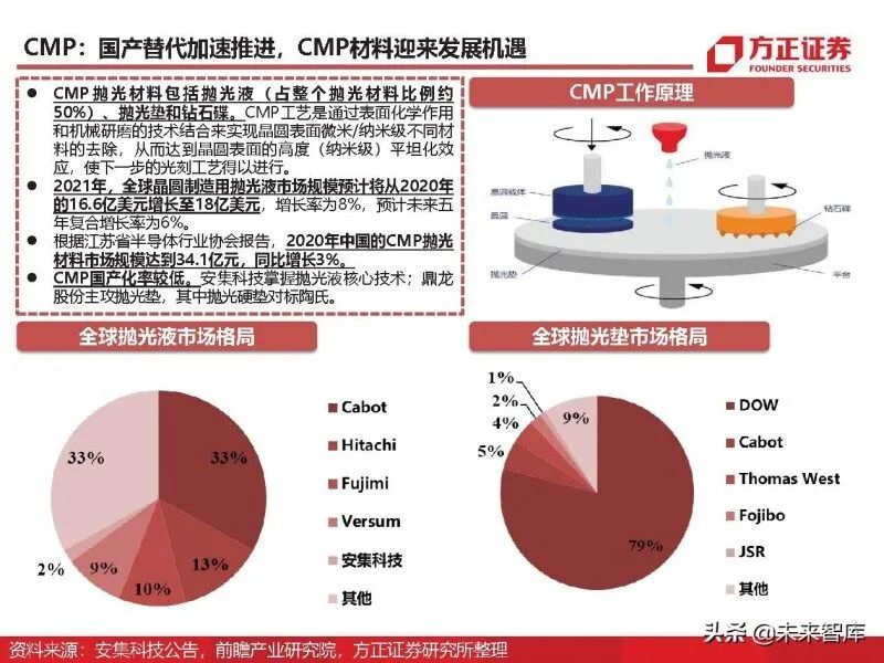
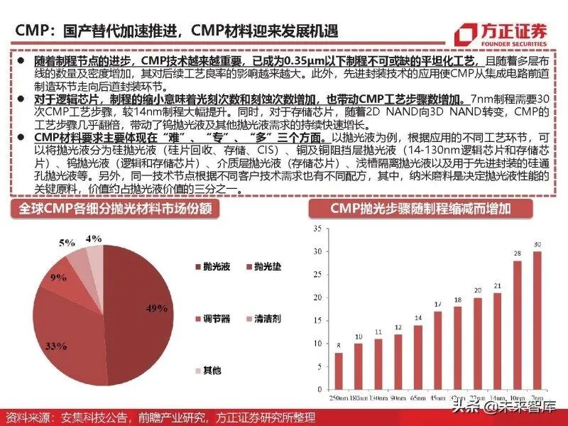
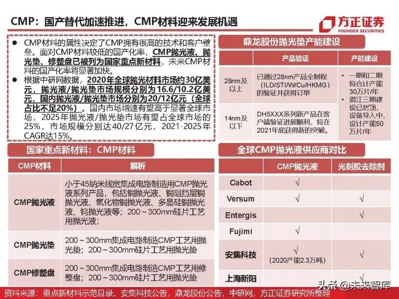
CMP: Accelerating Domestic Substitution, Development Opportunities for CMP Materials
CMP polishing materials include polishing liquids (accounting for about 50% of the total polishing materials), polishing pads, and diamond discs. The CMP process combines surface chemical action with mechanical grinding technology to achieve the removal of different materials at the micron/nanometer level on the wafer surface, thus achieving a high level of flatness (nanometer level) on the wafer surface, allowing the next step of the lithography process to proceed.
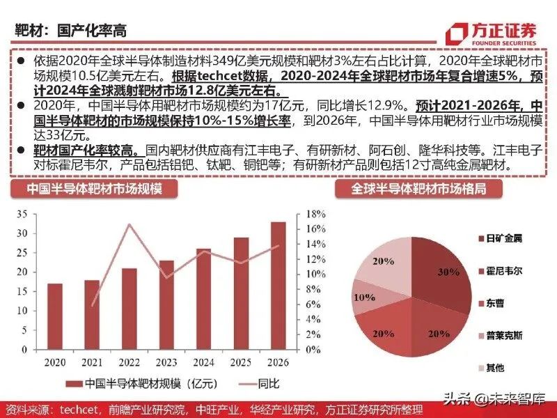
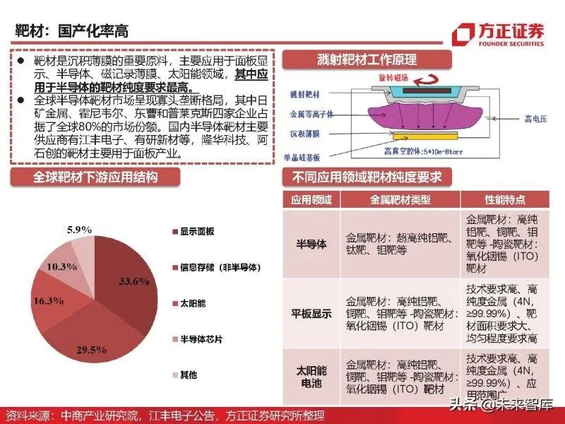
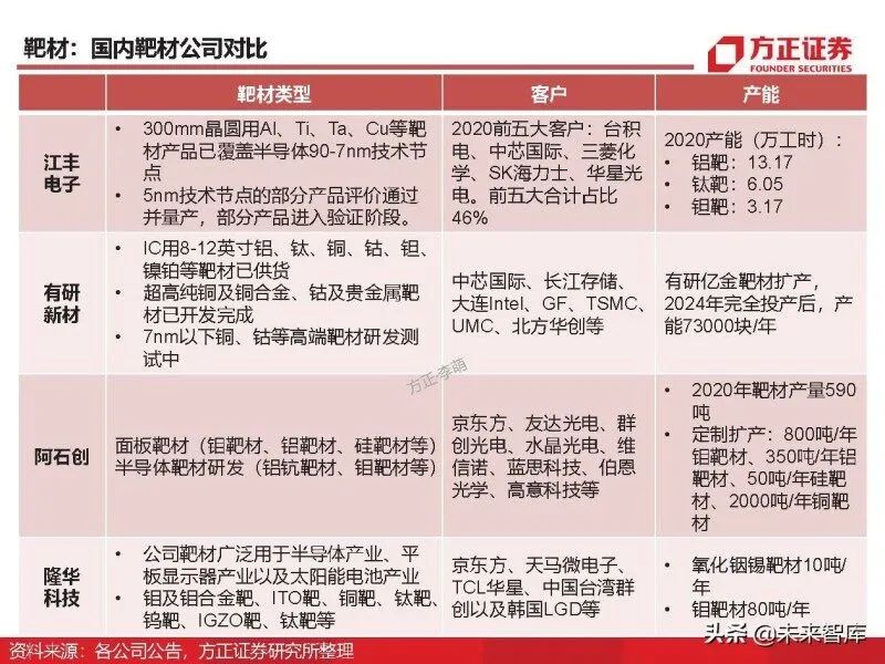
Target Materials: High Domestic Replacement Rate
Based on the global semiconductor manufacturing materials market size of $34.9 billion in 2020 and the approximately 3% share of target materials, the global target materials market size in 2020 was about $1.05 billion. According to Techcet data, the global target materials market is expected to grow at a compound annual growth rate of 5% from 2020 to 2024, with an estimated market size of $1.28 billion by 2024.
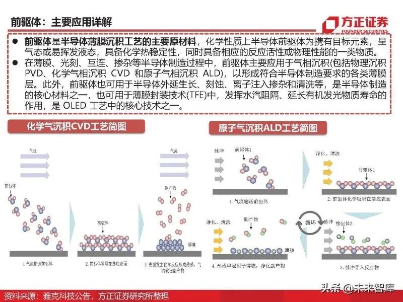
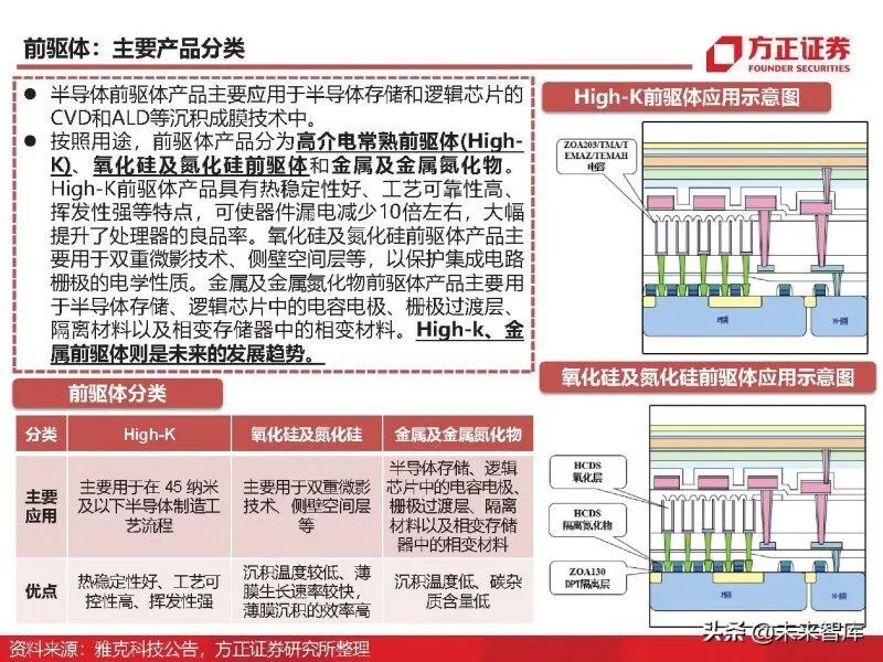
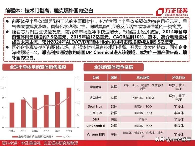
Precursors: Main Applications Explained
Precursors are the main raw materials for semiconductor thin film deposition processes, chemically characterized by carrying target elements in a gaseous or easily volatile liquid state, possessing chemical thermal stability, and having corresponding reactivity or physical properties.
Comparison of Semiconductor Materials and Equipment: Steady Demand Growth
As consumables, semiconductor materials have annual demand with overall steady growth, with volatility and cyclicality much lower than that of semiconductor equipment. Meanwhile, the global semiconductor materials market size maintains a relatively stable proportion of the semiconductor market size, remaining within the range of 11%-13%. (Report Source: Future Think Tank)
2. Three Catalysts Driving the Growth of Semiconductor Materials
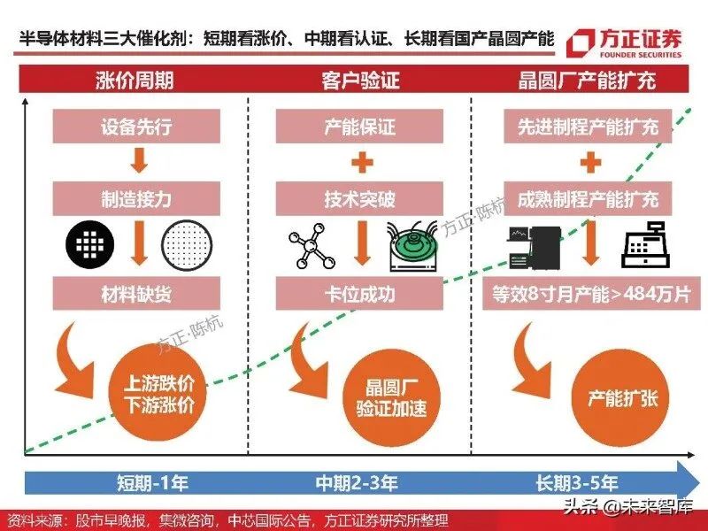
Short-Term Highlights of Semiconductor Materials: Price Increases
We believe that the prosperity cycle of semiconductors follows a common pattern of “equipment leading, manufacturing following, and materials shortages.” Considering that domestic wafer fabs have entered the expansion stage, and new capacities will be gradually opened in 2022, the expansion of wafer capacity will directly lead to a supply-demand imbalance in upstream materials, resulting in a cyclical “wafer crisis.” Global silicon wafer giant Shin-Etsu Chemical has already announced price increases, stating that it will raise prices for certain silicon products in April 2021. Additionally, Li Wei, Secretary of the Board of Directors of Shanghai Silicon Industry, stated at the SEMICON CHINA 2021 conference that some categories have seen price increases, not all, and the company’s silicon wafer orders have already exceeded supply capacity.
Logic of Semiconductor Material Substitution: Priority for New Production Lines in Wafer Fabs
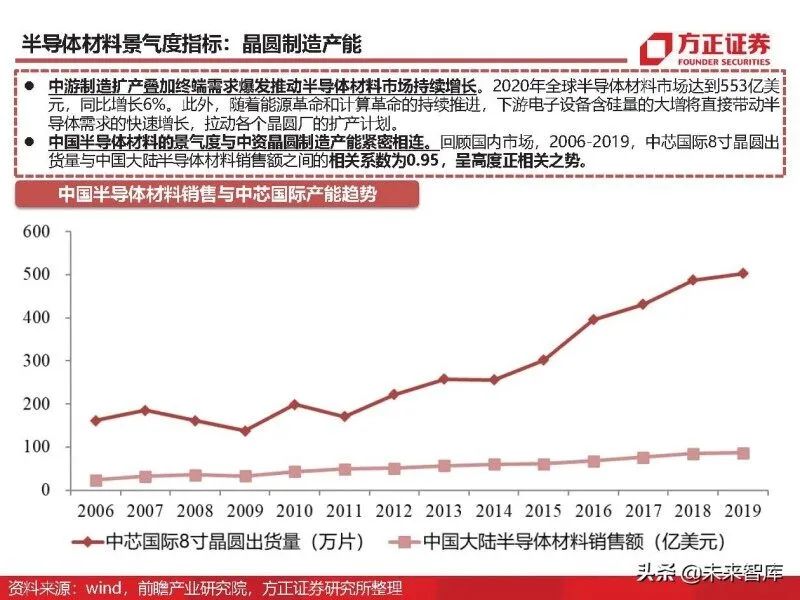
From 2012 to 2020, China’s share of the global semiconductor materials market steadily increased from 12.28% to 17.7%, ranking second globally. This is mainly due to: first, the continuous improvement of domestic enterprises’ technological levels, with some materials already achieving domestic substitution. Second, semiconductor materials are shifting to China along with the semiconductor industry, making China one of the main battlegrounds for semiconductor materials.
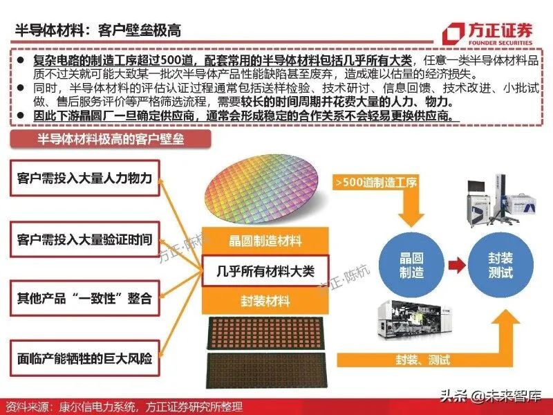
Mid-Term Highlights of Semiconductor Materials: Accelerated Verification
Generally speaking, the certification barriers for downstream semiconductor materials are high, and customer stickiness is significant. Customer certification barriers are the main factors hindering the development of domestic semiconductor materials, making it somewhat difficult for enterprises to achieve breakthroughs in the short term. Some companies may quickly enter related semiconductor material fields through mergers and acquisitions. Currently, very few companies can completely break through these barriers, and most segmented fields of materials are dominated by Japanese, Korean, and European and American companies.
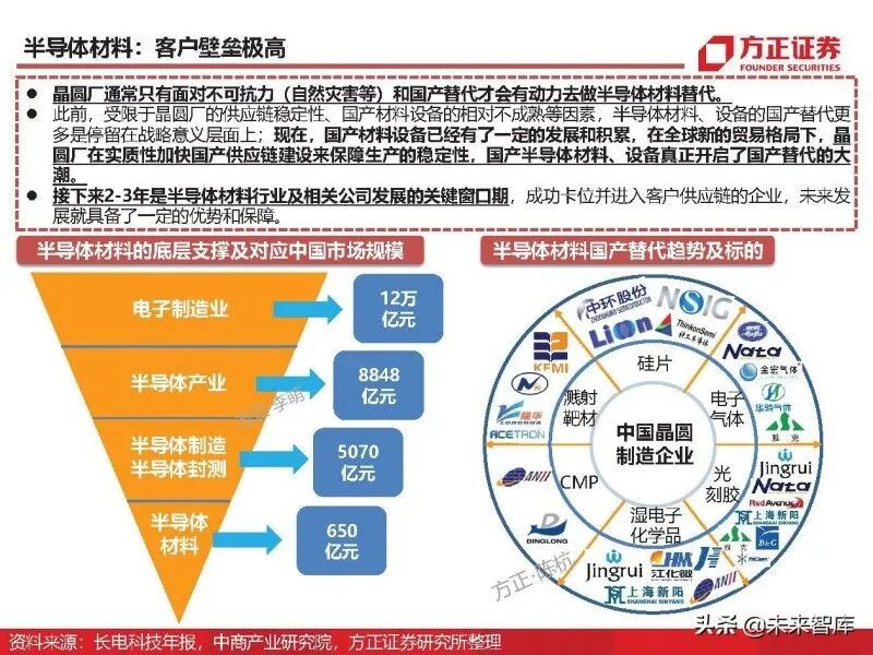
Long-Term Highlights of Semiconductor Materials: Expansion of Wafer Capacity
As discussed earlier, the revenue of China’s semiconductor materials is highly correlated with the capacity expansion of domestic wafer fabs, so the long-term development trend of China’s semiconductor materials depends on the pace of capacity expansion of domestic wafer fabs. According to IC Insights, it is estimated that in 2020, the market size of China’s wafer foundries increased by 26% year-on-year, reaching $14.86 billion, with domestic wafer fabs such as SMIC, Huahong Semiconductor, and Wuhan Xinxin accounting for only 25% of the domestic market share, indicating significant room for growth. In December of the same year, mainland China accounted for 15.3% of global wafer capacity, just 0.5% less than Japan.
3. Investment Outlook for Semiconductor Materials
Summary of Japan’s Semiconductor Materials Experience: Seizing Opportunities from Semiconductor Industry Transfer
In the 1970s, Japan leveraged its advantages in the home appliance industry to drive an overall upgrade in semiconductor technology, leading to the rise of a number of IDM companies and the first shift of the semiconductor industry from the United States to Japan. At that time, semiconductor memory, particularly DRAM, became Japan’s first industry. By 1986, Japanese semiconductor chips accounted for 40% of the global share, with DRAM reaching a maximum share of 80%, making it the focal point of global semiconductor chip manufacturing.
Summary of Japan’s Semiconductor Materials Experience: Combining Industry, Government, and Academia
In the 1970s, Japan’s Ministry of International Trade and Industry, along with Fujitsu, Hitachi, Mitsubishi, NEC, and Toshiba, established the VLSI joint R&D body, gathering national talent for collaborative research and development. The total project cost was 73.7 billion yen, of which 29.1 billion was government funding, accounting for 39.5%. During the four years of implementation, approximately 1,000 patents were obtained. The success of the VLSI project allowed Japan to gain an advantage in the field of ultra-large-scale integrated circuits, promoting the success of Japanese RAM.
The State Has Introduced Multiple Policies to Strongly Support Semiconductor Materials
The rapid development of China’s semiconductor materials cannot be separated from the support of relevant industrial policies. Special policies and large funds help the integration of upstream and downstream industries, and domestic wafer fabs have increased their willingness to certify domestic materials. Additionally, the second phase of the large fund has tilted more towards semiconductor manufacturing equipment and semiconductor materials to promote the comprehensive development of the entire semiconductor industry chain. In summary, China will seize the opportunities presented by this round of semiconductor industry transfer.
Investment Strategy for Semiconductor Packaging Materials
Advanced Packaging Continues Moore’s Law: The innovation process of Moore’s Law has achieved significant progress in semiconductor performance and cost: since the proposal of Moore’s Law in 1975, the number of transistors per wafer has increased by nearly 10 million, processor speeds have increased by 100,000 times, and the annualized compound cost of each transistor per wafer has decreased by 45%.
Advanced Packaging vs. Traditional Packaging: According to Yole data, the global packaging revenue has a compound annual growth rate of 4%. Among them, the advanced packaging market’s compound annual growth rate is 7%, and by 2025, advanced packaging revenue is expected to reach $42.2 billion, while traditional packaging’s compound annual growth rate is only 2%. As a result, the revenue share of global advanced packaging is expected to rise from 38% in 2014 to 49.4% by 2025.
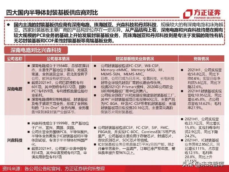
Packaging Substrates: Since the 1980s, the PCB industry has rapidly developed due to the IC design and manufacturing technology following Moore’s Law, leading to the emergence of micro semiconductor components and high-density multilayer packaging substrates, separating the integrated circuit packaging substrate from ordinary printed circuit boards and forming proprietary manufacturing technology for integrated circuit packaging substrates.
As a special printed circuit board, packaging substrates are the basic components that connect high-precision chips or devices with lower precision printed circuit boards. Compared to the 50μm/50μm parameters of PCB boards, packaging substrates can achieve parameters of <25μm/25μm. The overall refinement cost increase of PCB boards is much higher than the cost of interconnecting PCBs and chips through packaging substrates.
Packaging Substrate Market
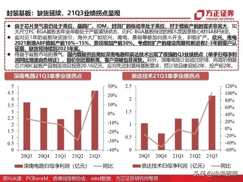
According to Prismark data, the global packaging substrate output value was $10.19 billion in 2020, a year-on-year increase of 25.2%. In the next five years, the compound annual growth rate of packaging substrates is expected to be 9.7%, reaching an output value of $16.19 billion by 2025. Shenzhen South Circuit is the largest domestic packaging substrate enterprise, with sales revenue of 1.544 billion yuan in its packaging substrate business in 2020, a year-on-year increase of 32.67%, but only accounting for 2.94% of the global packaging substrate market.
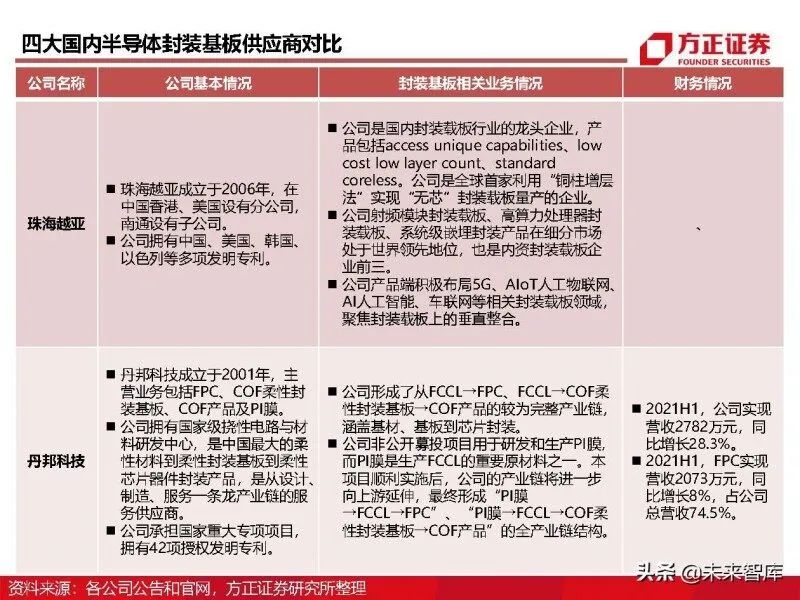
Packaging substrates originated in Japan and later extended to South Korea and Taiwan, with these three regions accounting for over 90% of the market share. In recent years, Japanese packaging substrate companies have gradually exited and scaled down, focusing on high-end products, with Japanese companies such as Ibiden, Shinko, and Kyocera having strong technical capabilities, occupying the main market for substrates required for CPU packaging, which have the highest profit margins in packaging substrates, while mass-produced substrates are mainly distributed in South Korea and Taiwan. In BGA packaging, the cost of substrates accounts for 40%-50%; in FC packaging, the cost of substrates accounts for 70%-80%.
Report Excerpt:
Produced by: Founder Securities Analyst: Chen Hang
CCTC®

Follow for moreClimate (Narrow/Wide) Info
Please long press to scan the QR code below
Follow Hua Xia Climate