(Source: Semiconductor Industry Observation)
One of the key technologies for achieving scaling below 3nm involves providing power from the backside of the chip. This novel approach enhances signal integrity and reduces routing congestion, but it also introduces new challenges for which there are currently no simple solutions.
Backside Power Delivery (BPD) eliminates the need to share interconnect resources between signal lines and power lines on the front side of the wafer. Instead, as the name suggests, power is transferred to the backside of the wafer, so only signals are transmitted via the front interconnects. Intel, Samsung, and TSMC have all announced plans to implement BPD in some form around the 2nm node.
In addition to eliminating RC bottlenecks, BPD can also save costs. Sanjay Natarajan, Intel’s Senior Vice President and Co-General Manager of Logic Technology Development, stated, “Backside power delivery eliminates the need for power rails in lower-layer front-end interconnects. This allows Intel to be less aggressive in interconnect scaling without skipping transistor density scaling. This enables less complex and ultimately cheaper lower metal patterning.”
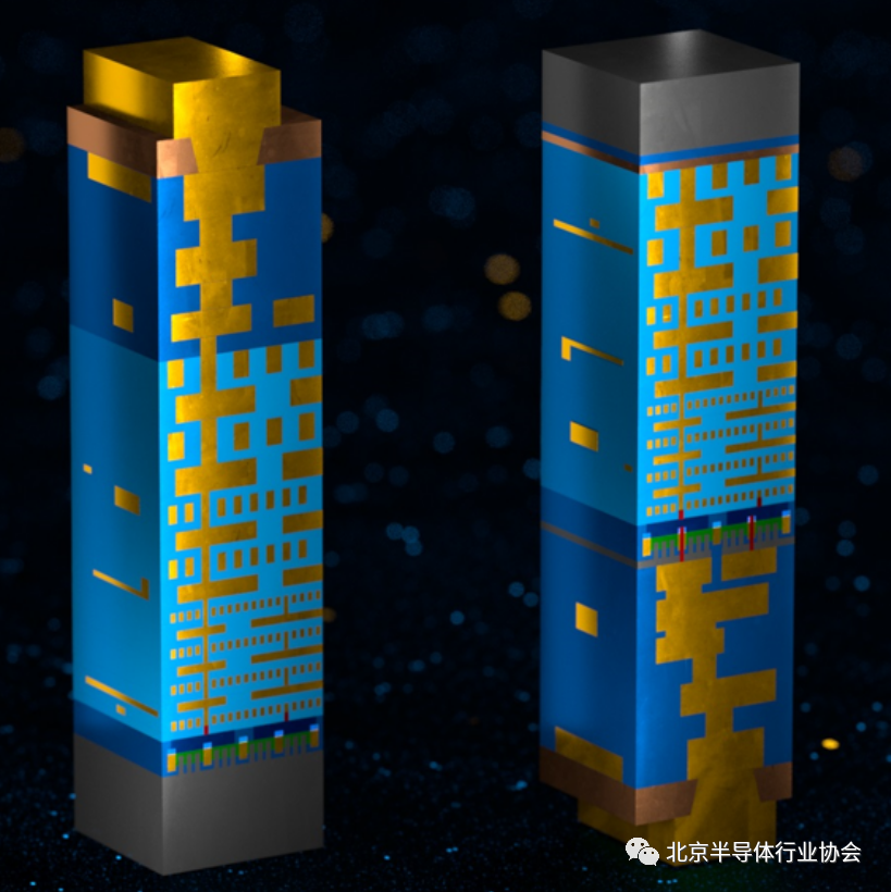
Figure 1: Interconnect layers of traditional logic devices (left) and a backside power delivery network using PowerVia (right). Source: Intel
It also allows for the optimization of manufacturing these different metal layers—as wider Vdd and Vss lines, as well as thinner lines for signal transmission. Nevertheless, the backside power network presents significant wafer processing challenges—especially since this change may occur at the same node where device manufacturers transition from finFET to nanosheet transistors.
For example, Intel will introduce RibbonFET and PowerVia at its 20A (2nm) node. “The first key challenge around PowerVia involves patterning electrical contact features in the tight space around the next-generation RibbonFET transistors without impacting their performance. The second is thinning the backside silicon to provide as direct and low-resistance a connection as possible in a repeatable and controllable manner,” Natarajan said.
As the BPD approach is very new, the industry is weighing the pros and cons of different architectures.
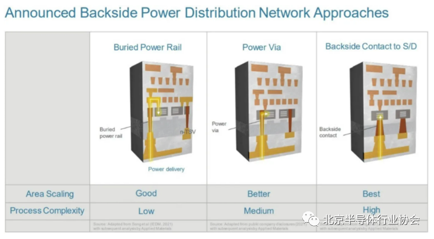
Figure 2: BPD schemes provide different scaling advantages associated with increased wafer processing complexity. Source: Applied Materials
BPD Schemes
An ideal power delivery network provides a constant, stable power voltage to active circuits on the IC during any activity. “The key parameter is the DC resistance of the PDN across all interconnect paths, from the IC’s power pins to the transistors in the circuit.”
Figure 2 shows three implementations of the backside power delivery network. “In the first approach, the logic units retain power rails, and the backside distribution network connects to the power rails via nano TSVs,” said Mehul Naik, Managing Director at Applied Materials. “In the second approach, there are no power rails in the logic units. Instead, power vias directly transfer power from the backside network to the cells or transistor contacts. This method is more complex but improves power efficiency and increases unit area scaling. In the third approach, power from the backside network is directly connected to the source and drain of each transistor.”
Imec is one of the earliest companies to develop backside power delivery methods, using what is called embedded power rails (BPR). “If we do a backside power delivery network, we also have embedded power rails, with a via from the source/drain area to that BPR. So we have TSVs going through the silicon and landing on the buried power rails, but the buried power rails are made even before the transistors are manufactured. They are located between the nanosheet fins before the gate formation and before the source/drain epitaxy is completed,” explained Eric Beyne, Senior Researcher, Vice President of R&D, and Director of the imec 3D System Integration Project. “This is one of the reasons why copper will never be used here. It has to go through all the front-end processing, so it must be compatible—like tungsten or molybdenum.”
Integrating these into the manufacturing process itself is a challenge. “These power rails are made during the process of defining the fins or sheets, where the space between the fins is maximized because once you deposit the gate and metal, the fins get thicker, and the spacing between two adjacent fins becomes very narrow,” Beyne said. “So you have to make very deep vias with smaller feature sizes.”
He noted that the short vias to the buried power rails can be located in the tight spaces along the BPR, providing good performance advantages.
BPR is parallel to the fin direction, partially buried in shallow trench isolation and partially in the silicon substrate. This is different from traditional grids with power rails in M0 or M1, which can reduce the height of standard cells.
Natarajan said, “Intel’s PowerVia provides a more direct, single-function connection between the backside power delivery network and traditional source contacts, and we believe it can achieve lower resistance compared to the imec method.”
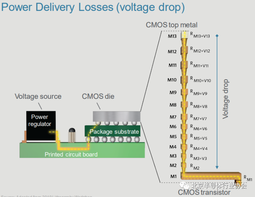
Figure 3: Power delivery network design margins allow for a 10% IR drop. Higher levels may threaten device performance. Source: Applied Materials
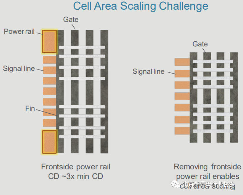
Figure 4: By moving the power rails, the area of standard cells can be expanded by 20% to 30%. Source: Applied Materials
Why Backside Power Delivery, and Why Now?
The reason for this significant change in how power is delivered to transistors relates to voltage (IR) losses, as electrons must traverse 15 or more layers of interconnects and vias to deliver power and data to the billions of transistors in modern SoCs. Power efficiency can reach a specification limit of 90%, or a 10% voltage (IR) loss between the chip regulator and its transistors (see Figure 3).
In backside power delivery, the power rails are moved out of the logic units, thereby increasing logic density. Applied Materials estimates this is equivalent to two generations of lithography scaling (see Figure 4). Since power is delivered directly from beneath the transistors, the IR drop is significantly reduced.
Simulations and manufacturing studies conducted by Arm and imec have determined that if the distance between nano TSVs is less than 2µm, the efficiency of backside power delivery can be seven times that of front power delivery networks.
However, some process and material changes must be implemented to make BPD a reality in production fabs. “To better utilize area and improve performance, backside power delivery (BPD) networks are an attractive option. Tomonari Yamamoto, Vice President of Equipment Technology at TEL Corporate Innovation Division, stated, “To achieve this, continuous process and tool improvements are needed not only in thin films, etching, lithography, and wet processes but also in wafer bonding and thinning technologies.” In fact, many lower-resistance metals are being evaluated as potential candidates to replace copper, which will be necessary as BEOL interconnect CDs delve below 15nm.
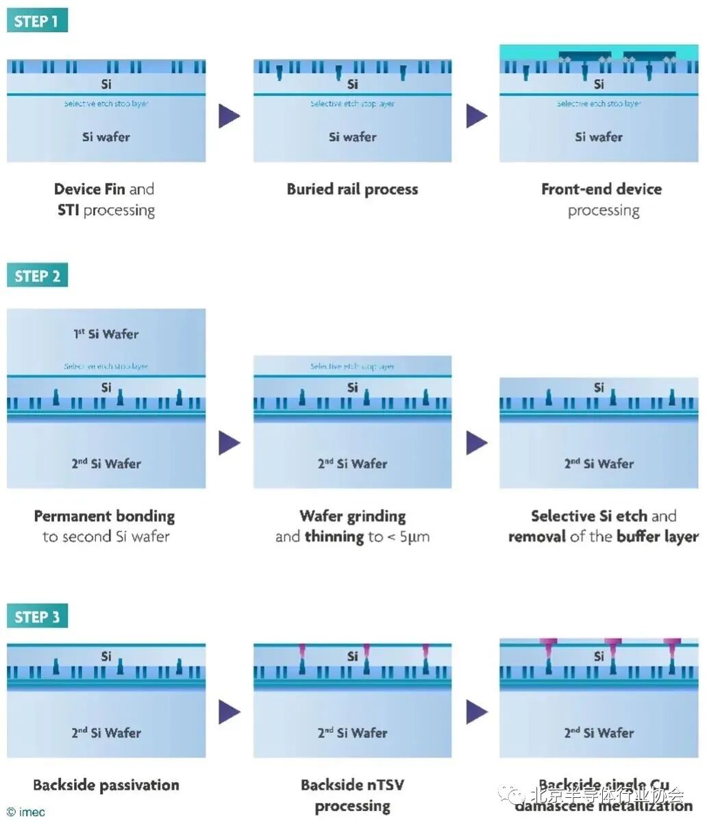
Figure 5: The backside power delivery network process requires extreme thinning of the wafer to <500nm on a 50nm SiGe layer with a 350nm silicon epitaxial cap. The resistance of embedded ruthenium power rails is 40% lower than tungsten rails. After wafer bonding comes thinning, CMP, dry and wet etching, followed by TSV and M1 formation. Source: imec
Embedded Power Rails and BPD
The imec process flow (see Figure 5) starts with the epitaxial growth of SiGe, followed by a silicon capping layer. A high Ge concentration (25%) improves the selectivity of CMP stopping on the thin film. Then, long buried power rails are etched in STI and extended into the silicon. Imec compared tungsten and ruthenium CVD films, with the latter showing a 40% reduction in resistance. The wafers are then permanently bonded to a carrier wafer using SiCN-SiCN dielectric bonding. The wafers undergo backside grinding and CMP, followed by dry and wet etching. SiGe is removed by chemical etching.
The wafer bonding process must be executed carefully to minimize distortion that could interfere with subsequent patterning steps. “When you do bonding, the pattern after bonding is likely to distort, and the backside pattern must correct for that distortion,” Beyne said. “It may not be much, but even at a 1ppm scaling factor, with a temperature increase of no more than 1°C, you can expand the silicon and potentially create a 150nm misalignment at the wafer edge.”
Next, the nano TSV process begins with oxide deposition (LPCVD), followed by self-aligned DUV patterning. Advanced lithography correction methods reduce the 100nm overlap in the x and y directions to 10nm. Bosch etching tools create high AR nanoTSVs that land on the BPR oxide and STI. Next, PECVD oxide is deposited inside the nano TSVs, followed by sputter etching of the BPR to ensure good contact between the nano TSVs and BPR. After TiN ALD comes W CVD and W CMP. Then copper is plated to form the backside metal (see Figure 6).
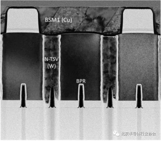
Figure 6: TEM cross-section of a passive test structure shows backside copper foil landing on buried power rails with 90nm nanoTSVs. Source: imec
Beyne noted that other difficult challenges include backside patterning and accurately aligning power rails with standard cell sizes. Although the state-of-the-art overlay tolerance for EUV lithography is about 3nm, there are distortion issues associated with wafer bonding on the backside, with an overlay tolerance range of about 20nm.
“Of course, you encounter all the usual challenges in interconnect processing, creating high aspect ratio dimensions, depositing thin liners, and void-free barrier layers,” he said.
Importantly, if like all fabs today, transistors are processed first, there is no necessity to adopt new interconnect metals at the 2nm node. In fact, Intel’s PowerVia seems to allow just that. “The PowerVia process we designed is compatible with traditional front-end contact metals, including tungsten, and advanced metal processes to optimize the performance of PowerVia,” Natarajan said.
Naik described the backside power delivery network as a form of Design Technology Co-Optimization (DTCO), where design and process innovations can yield system-level advantages. He emphasized the thermal limitations present when constructing backside nanoTSVs.
“We need to design the backside contacts of the transistor source to have as low resistance as possible,” Naik said. “This often requires high-temperature epitaxy and annealing processes. However, since the backside contacts are made with the front transistors and interconnects in place, they can degrade due to these high temperatures. To address this, Applied is developing a low-temperature solution that combines up to seven steps in high vacuum, including pre-cleaning, selective silicide deposition, ALD or PVD liner deposition, and new metal filling chambers. The co-optimized CMP step leaves a perfectly uniform backside contact layer on which we can build the copper backside power delivery network.”
Providing sufficiently isolated deposition films for the transistors from the power network and etching steps close to the active regions of the transistors will require precise engineering design. David Fried, Vice President of Product at Lam Research, stated, “In etching, regardless of the process flow, you need high anisotropic, defect-free, and damage-free results. In deposition, everything depends on the material parameters you are depositing. You need low defect rates, high yields, and the ability to design these materials.”
Once companies do transition to backside power delivery networks, it is important that the method can also scale to the next process node. “Our standard cell pitch is 105nm, and if you connect the nanoTSVs to every other embedded power rail, there will be a connection every 210nm—so 200nm lines and 200nm pitches. This separates from standard cell separation, so if you scale down to 80nm, it will still work, and you don’t have to do EUV lithography on the backside in that case,” Beyne said.
Subsequent Steps to Minimize RC Delay
Since the 22nm device generation, BEOL RC delay has accounted for a larger portion of total device delay as transistors continue to shrink. For copper plating methods, via copper filling has become increasingly challenging and requires improvements in ultra-thin wetting and capping CVD processes.
“For copper, we can reduce to around 200nm, but you need a copper seed layer for plating. For nano TSVs, using ALD and CVD materials, tungsten and other metals scale better in high aspect ratio structures, but you still need TiN barrier metals, such as for tungsten. At some point, you have more barriers than bulk metals, like 30nm sizes,” Beyne said. “Molybdenum is very attractive for some of these TSV applications because it is ALD and it directly deposits on the surface. I would say tungsten is the most common material today. Improved options include ruthenium and molybdenum, but they are still in the research phase.”
Yamamoto from TEL shares a similar view. “Ruthenium is a candidate material because it is less sensitive to scattering and does not require thick barrier metals, just an adhesion layer of less than 1nm thickness.” He added that plating processes tend to provide a 2:1 aspect ratio, while subtractive etching schemes can achieve higher aspect ratios, which will reduce resistance while controlling the increase in capacitance, for example, by replacing low-k films with air gaps.
Conclusion
Optimizing the interconnect performance of the backside network is somewhat similar to that of the front network—ensuring low resistance and long-term reliability of the backside metal. However, Natarajan pointed out that by separating the power routing on the backside metal stack from the signal routing on the front metal stack, engineers can freely optimize resistance and capacitance independently. Companies may also make different architectural choices based on performance needs, such as dual plating processes versus subtractive processes (metal deposition and etching).
Leading equipment manufacturers will adopt backside power delivery in 2nm designs, ensuring cleaner power delivery and breaking the RC bottleneck. Comprehensive advancements in deposition, etching, CMP, bonding, wafer thinning, and DTCO will influence this inflection point.