Online debugging (OCD, On-Chip Debugging) interfaces provide chip-level control over target devices, serving as a primary means for engineers, researchers, and hackers to extract firmware code or data, modify memory contents, or change device operations. If you are familiar with hardware circuits or embedded systems, you certainly know that JTAG (Joint Test Action Group) and UART (Universal Asynchronous Receiver/Transmitter) are among the most widely used serial communication interfaces.
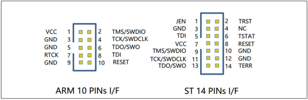
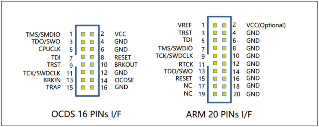
The JTAG specification does not have a standard interface definition, so you can find 4-20 pin JTAG headers on various PCB hardware, and the function definitions of each pin are also uncertain, which causes significant troubles for debugging work. The following figure lists four types of interface definitions, including those from ARM and ST companies.
So how can we know the pin definitions? The traditional approach is to use a logic analyzer for signal analysis, which is both time-consuming and error-prone. Thus, devices for automatic identification of JTAG interfaces have emerged, such as JTAGulator, JTAGenum, JTAG Finder, JTAG Pinout Tool, etc. Currently, the most user-friendly is still JTAGulator.
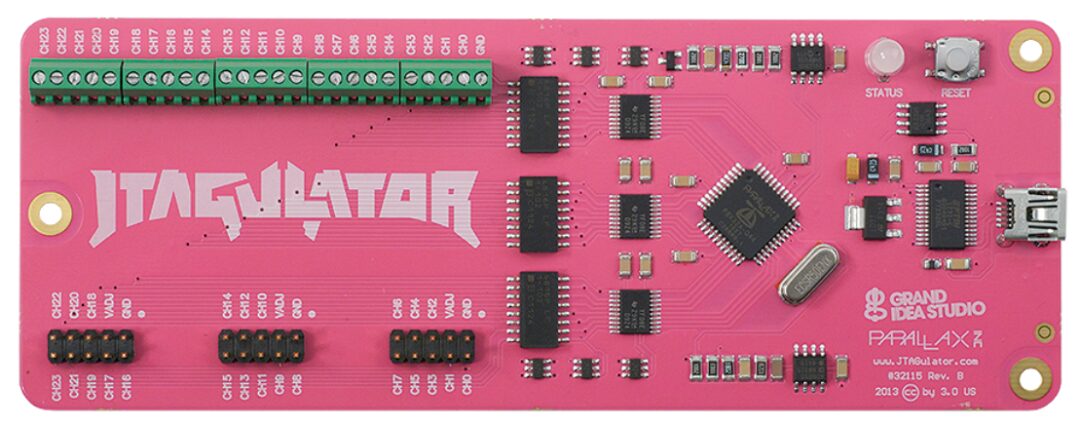
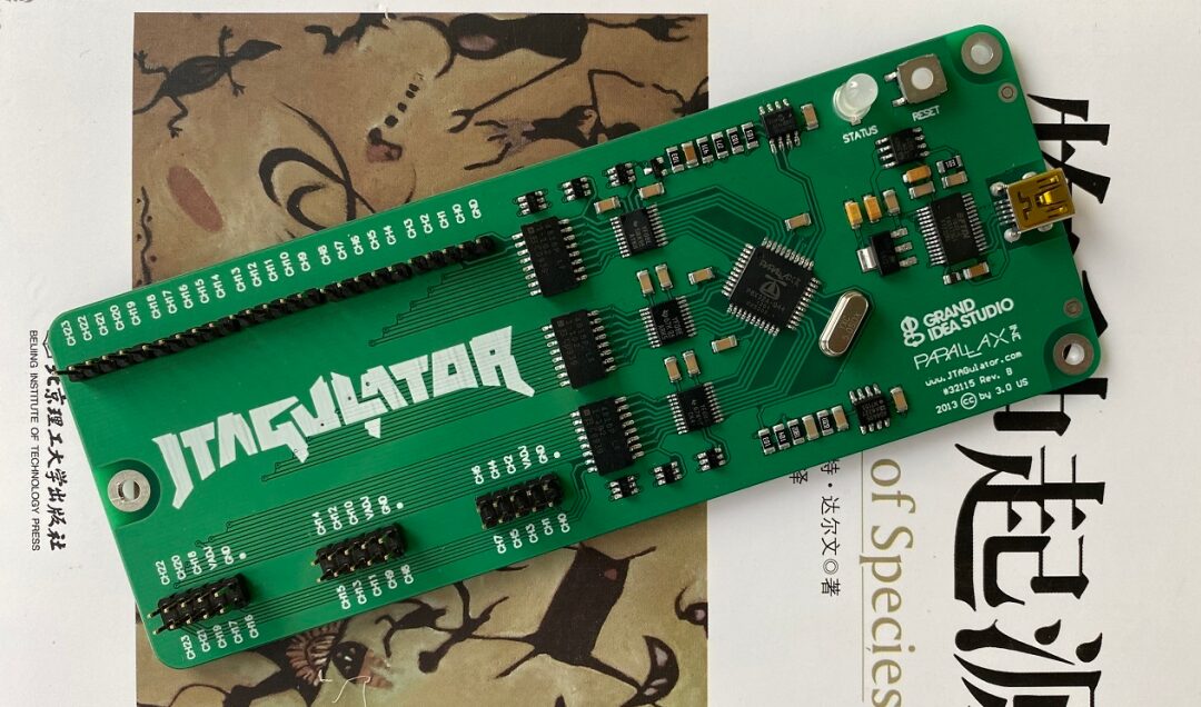
JTAGulator is an open-source hardware tool that can be used to identify OCD connections at test points, vias, or component pads on the target device, allowing for the use of the Attify Badge for wiring and reading firmware.
JTAG stands for Joint Test Action Group, which is a common name for the IEEE standard 1149.1 known as the Standard Test Access Port and Boundary Scan Architecture. This standard is used to verify the functionality of printed circuit boards designed and tested in production.
JTAG was officially standardized in 1990 by IEEE document 1149.1-1990, and in 1994, a supplementary document was added to explain the Boundary Scan Description Language (BSDL). Since then, this standard has been widely adopted by electronic companies worldwide. Boundary scan has almost become synonymous with JTAG.
The three main functions of JTAG are:
-
Downloader, that is, downloading firmware to the device’s FLASH chip.
-
DEBUG, similar to a doctor’s stethoscope, can probe internal chip errors.
-
Boundary scan, which can access the logical states of internal chip models and the states of chip pins, etc.
In JTAG interfaces, the most commonly used signals are five: TCK / TMS / TDO / TDI / TRST, of which four are input signal interfaces, and one is an output signal interface.
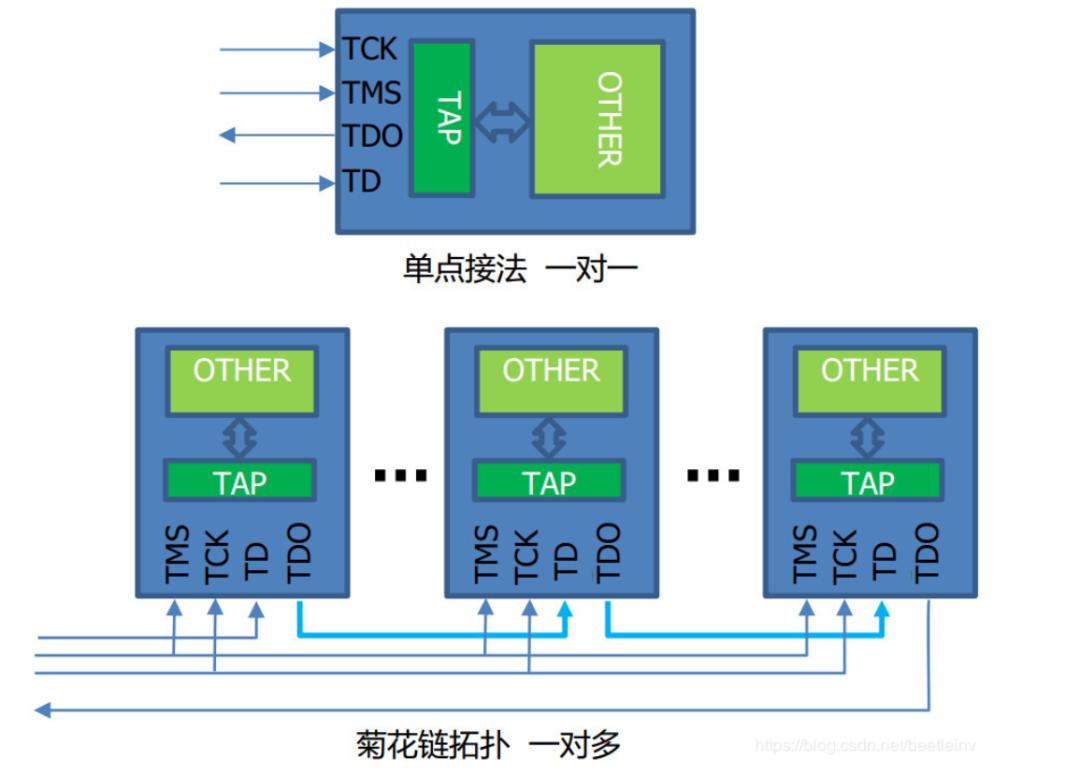
JTAG was initially used for testing chips, and its basic principle is to define a TAP (Test Access Port) inside the device and specify the behavior of the TAP state machine, allowing internal nodes to be tested through dedicated testing tools. JTAG testing allows multiple devices to be connected in series through the JTAG interface, forming a JTAG chain, enabling individual testing of each device. Now, the JTAG interface is also commonly used for implementing ISP (In-System Programmable) for programming devices like Flash. Below, we introduce these five interfaces:
-
Test Clock Input (TCK)TCK is mandatory in the IEEE1149.1 standard. TCK provides a separate, basic clock signal for the operation of the TAP, and all operations of the TAP are driven by this clock signal.
-
Test Reset Input (TRST)This signal interface is optional in the IEEE 1149.1 standard and is not mandatory. TRST can be used to reset (initialize) the TAP Controller. Since the TAP Controller can also be reset (initialized) through TMS, this leads to the distinction between four-wire and five-wire JTAG.
The JTAG interface can be used one-to-one or form a daisy chain in a one-to-many topology. The two topologies are shown in the figure below. In multi-core chips, the internal connections are already made in a daisy chain format.
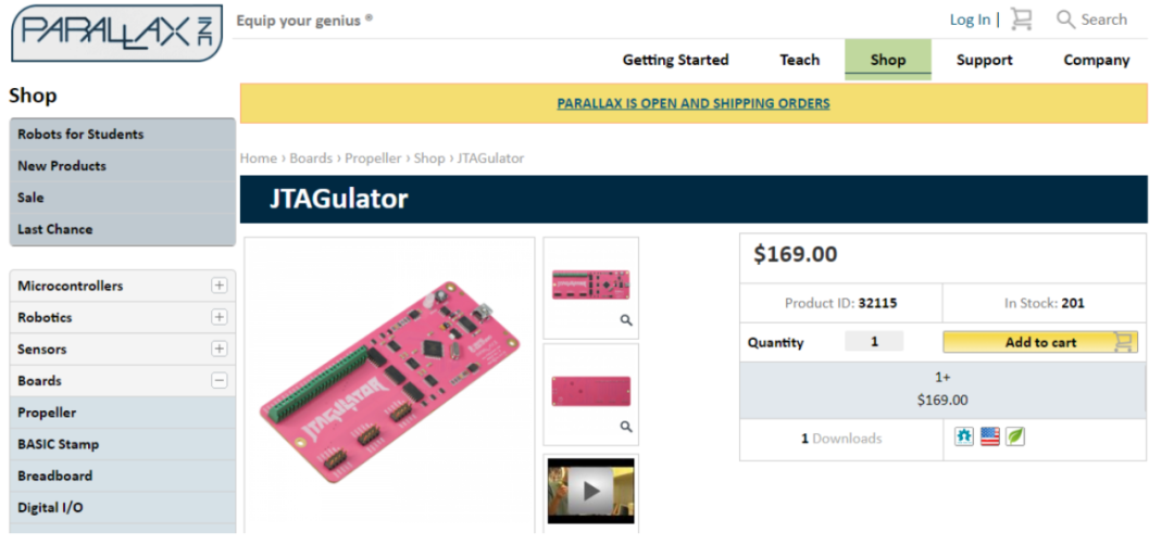
The official price of JTAGulator is $169, while the purchasing price on Taobao is around 1500 RMB. The DIY cost can be controlled within 500 RMB per board.
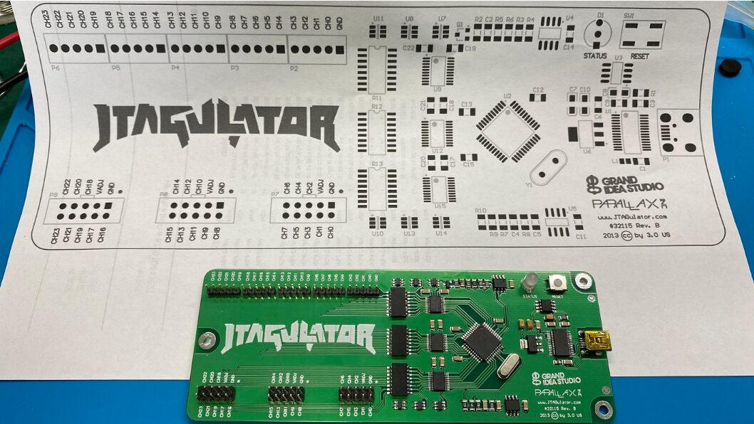
All the materials needed to make the JTAGulator can be downloaded from the official website, including GERBER files, BOM component lists, etc.

Send the GERBER files to a factory for PCB prototyping, and it will arrive in 2-3 days. Then purchase the electronic components listed in the BOM. I prototyped the PCB at Jialichuang and purchased the electronic components at Lichuang Mall.
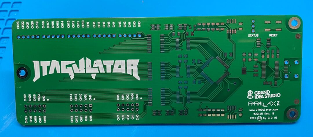
According to the PCB assembly diagram provided on the official website, solder the electronic components onto the PCB using a soldering iron and solder. After soldering, clean the residue of flux and soldering aid with cleaning fluid, and carefully check for cold solder joints and short circuits before powering on.
Connect the computer using a Mini USB data cable, and you will see a serial communication port in the “Device Manager”.
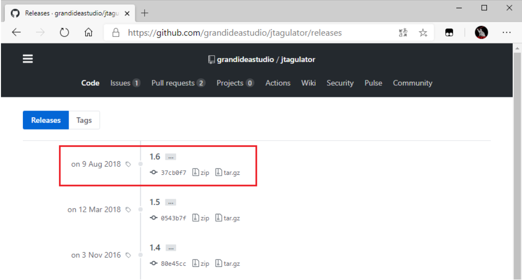
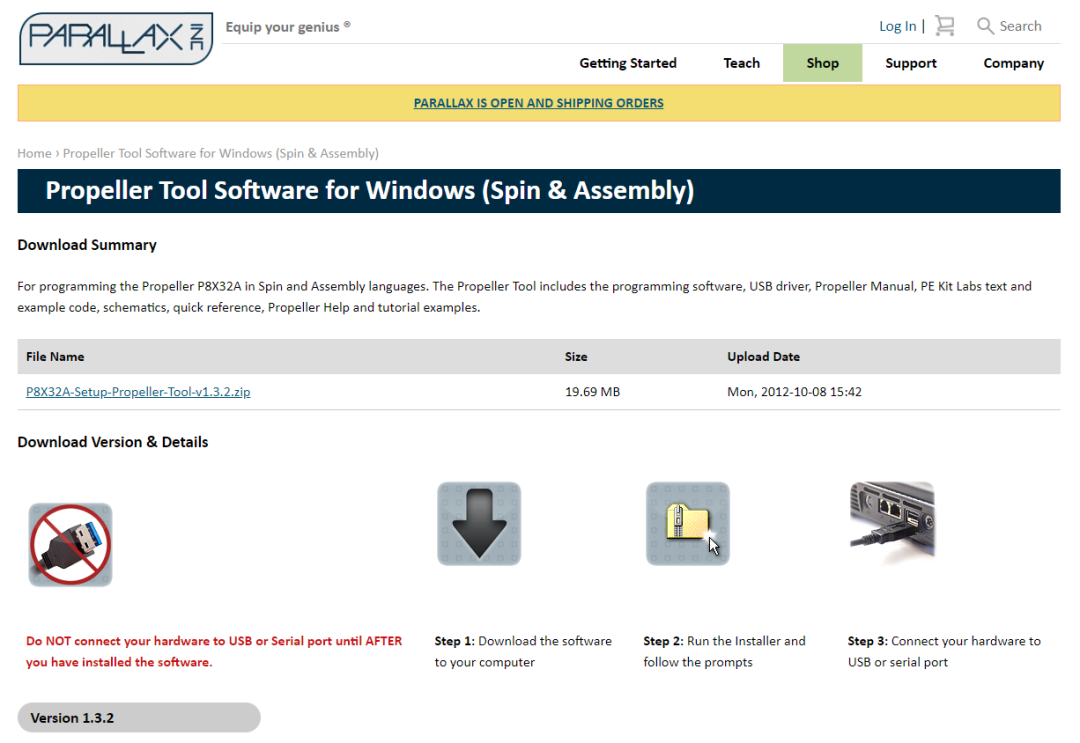
After confirming that the hardware is working fine, download the firmware source code from GitHub, and install the programming tool Propeller Tool required for programming the chip.
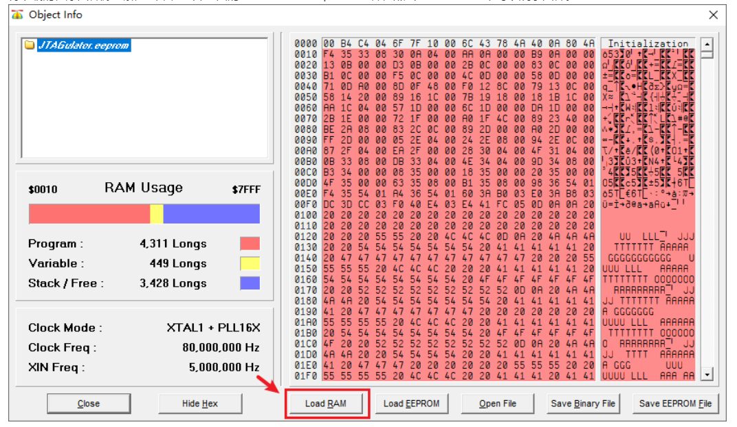
Extract the downloaded firmware source code, open the “JTAGulator.eeprom” file inside, and click “Load ARM” to program the firmware onto the board.
After programming, open the corresponding COM port of the JTAGulator using a serial debugging tool, set the baud rate to 115200, press the enter key, and the returned data will be displayed. Press “H” to view help and “I” to check the version.
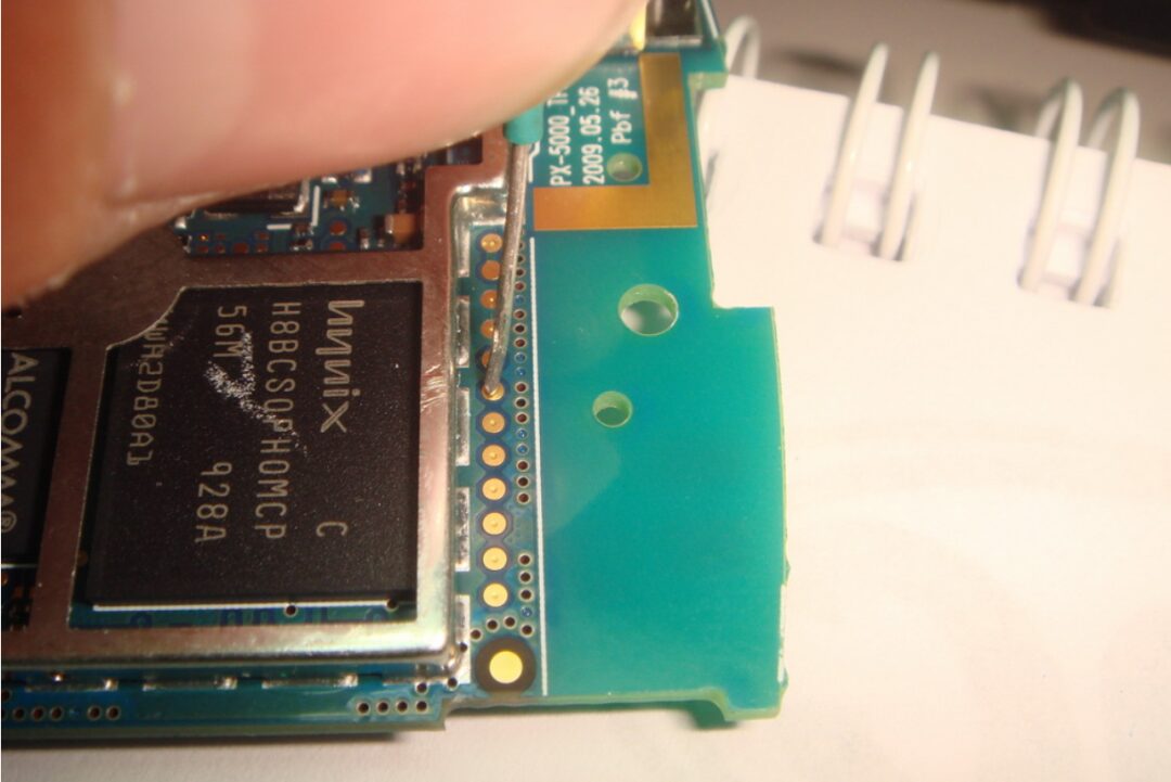
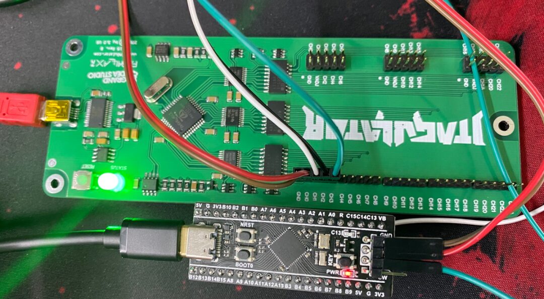
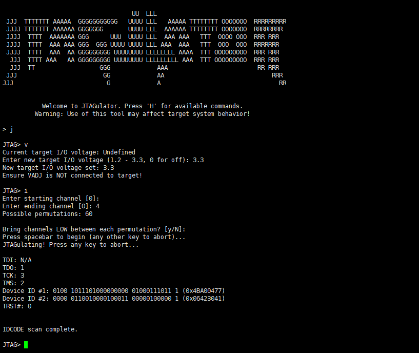
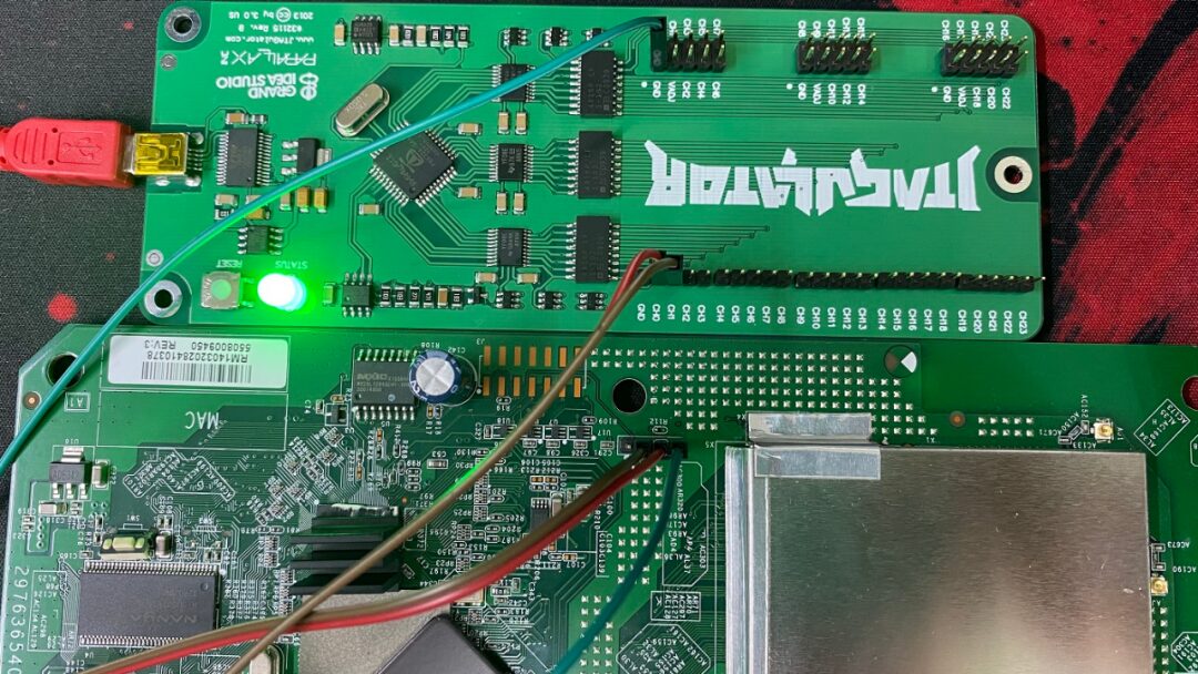
Use an STM32 development board for testing, pretending not to know its pin definitions. Power the board separately, first use a multimeter to measure the GND pin, and then connect the pins to be identified and the GND pin to the JTAGulator using DuPont wires.
Input “J” to enter JTAG mode, “V” to set the voltage, “I” for IDCODE scanning, then set the channel range to successfully identify the pin definitions.
Use a Netgear router for testing, following the same steps: first use a multimeter to measure the GND pin, then connect the remaining pins to the JTAGulator.
Successfully identified the TX and RX pins.
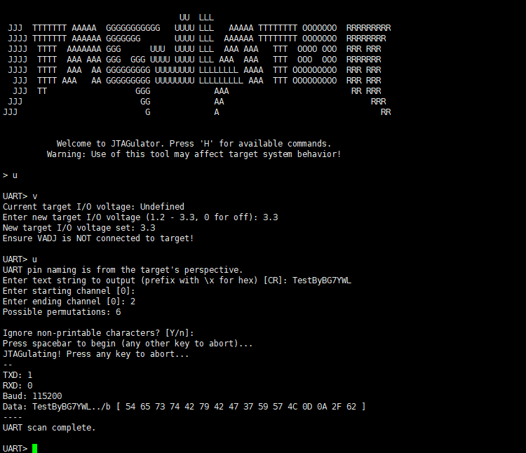
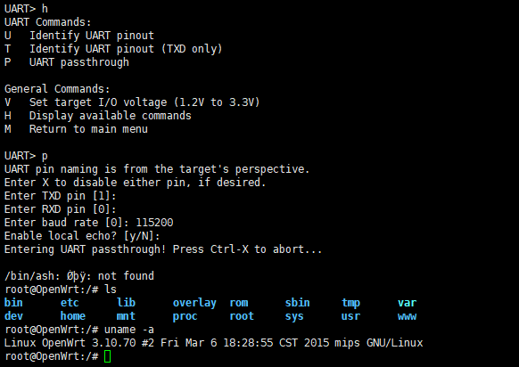
You can also use JTAGulator to debug the router via the UART serial port.
JTAGulator can quickly identify which pins may be JTAG and find the order of these pins. Here, I would like to thank the author Joe Grand for open-sourcing this hardware tool.
Friends who cannot DIY can try another cheaper solution, JTAGenum, which can be programmed using an Arduino Nano development board or Raspberry Pi.
The difference between JTAGulator and JTAGenum is that JTAGulator has built-in level shifting and input protection. In terms of software, JTAGulator provides UART scanning, which JTAGenum currently does not support, and JTAGulator also provides the functionality to scan unrecorded JTAG interfaces, which JTAGenum currently does not support.
Lenovo Global Security Lab “Building and Reading Firmware with JTAGulator (Part 1)”
http://www.grandideastudio.com/jtagulator/
https://github.com/grandideastudio/jtagulator
https://blog.csdn.net/beetleinv/article/details/86372466