Title: Briefly describe the ASIC design process and list the tools used in each part.
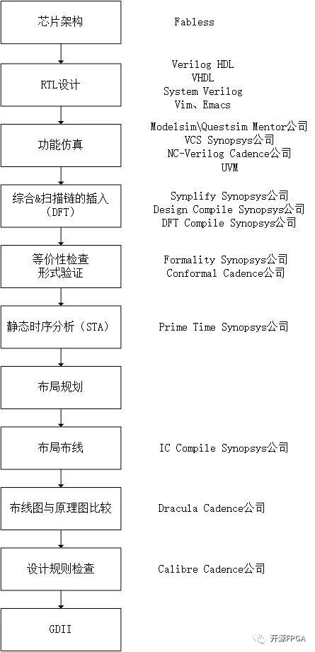
Basic ASIC Development Process
Chip Architecture, considering chip definition, process, and packaging.
RTL Design, described using Verilog, System Verilog, or VHDL.
Functional Simulation, simulation under ideal conditions.
Verification, using UVM verification methodology and FPGA prototype verification.
Synthesis, logic synthesis, mapping the described RTL code to basic logic gates and flip-flops.
DFT Techniques, inserting scan chains.
Equivalence Checking, using formal verification techniques.
STA, Static Timing Analysis.
Layout Planning, ensuring minimal internal interactions to avoid congestion and issues in routing.
Clock Tree Synthesis, evenly distributing the clock to reduce clock skew between different parts of the design.
DRC, Design Rule Check.
LVS, comparing the layout and schematic.
Generate GDSII.
This entire process is referred to as RTL2GDSII, and the process of using GDSII to produce chips is called tape-out. The above is a simplified design process for a Fabless company, which ultimately sends the GDSII to a foundry for chip production.
Title: Briefly describe the FPGA development process.
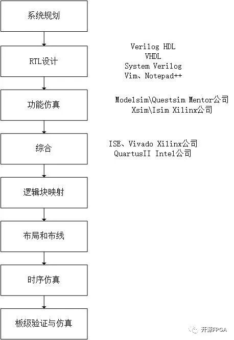
Basic FPGA Development Process
System Planning, system functionality and functional module division.
RTL Design, described using Verilog, System Verilog, or VHDL.
Functional Simulation, simulation under ideal conditions.
Synthesis, Compilation, Layout, and Routing, completed using tools provided by FPGA vendors.
Timing Simulation, timing analysis constraints.
Board-Level Verification.
Must give a thumbs up!!