Source: https://www.cypress.com/
Translated and organized by RF Academy, for learning purposes only.
Hello everyone, this is 【RF Academy】.
Today we will learn together about Cypress’s “Antenna Design and RF Layout Guide.” If you need the original document, please leave a message at the end.
This guide explains antenna design in simple terms and provides guidelines for selecting RF components, designing matching networks, and layout design. This application note also recommends two PCB antennas tested by Cypress, which can be realized at a very low cost for use with low-power Bluetooth (BLE) solutions in the Cypress PSoC® and PRoC® series. The PRoC BLE, PSoC 4 BLE, and PSoC 6 BLE 2.4-GHz radios must be carefully matched with their antennas for optimal performance.
Let’s briefly review the main knowledge points of the guide.
Antenna design and RF layout are key components in wireless systems, responsible for sending and receiving electromagnetic radiation from the air. The wireless range obtained by end customers from an RF product (such as a coin-sized battery) mainly depends on the antenna design, housing, and good PCB layout. It is also normal for systems with the same chip and power but different layout and antenna design practices to have significant variations in RF range. This application note introduces best practices, layout guidelines, and antenna debugging procedures, and provides the widest bandwidth achievable with a given power. RF tracing, power decoupling, via holes, PCB stacking, and overall layout considerations for the antenna and ground are also discussed. The application note also details the selection of RF passive components (such as inductors and capacitors). Each topic ends with tips or checklists related to the subject.
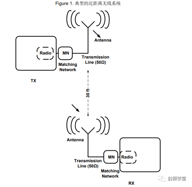
Figure 1 shows the key components of a wireless system on the transmitter (TX) and receiver (RX).
A well-designed antenna can extend the operational range of wireless products. The greater the energy sent from the wireless module, the further the transmission distance under fixed data packet error rate (PER) and receiver sensitivity conditions. Similarly, a well-tuned radio on the receiver side can operate under minimal radiation conditions on the antenna. RF layout, along with the wireless matching network, needs to be correctly designed to ensure that most of the power from RF reaches the antenna and vice versa.
undefined
An antenna generally refers to a conductor exposed in space. When the length of the conductor is in a specific proportion or integer multiple to the signal wavelength, it can be used as an antenna. Since the electrical energy supplied to the antenna is radiated into space, this condition is referred to as “resonance.”
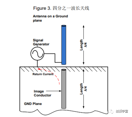
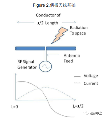 As shown in Figure 2, the wavelength of the conductor is Lambda/2, where Lambda is the wavelength of the electrical signal. The signal generator powers the antenna at its center point through a transmission line (also known as antenna feed). This length will create voltage and current standing waves along the entire conductor, as shown in Figure 2. The electrical energy input to the antenna is converted into electromagnetic radiation and radiated into the air at the corresponding frequency. The antenna is powered by the antenna feed, which has a characteristic impedance of 50 Ω, and radiates into space with a characteristic impedance of 377 Ω. Therefore, there are two very important considerations for the geometry of the antenna: 1. Antenna length 2. Antenna feed. An antenna of length Lambda/2 (as shown in Figure 2) is called a dipole antenna. However, in printed circuit boards, the length of conductors used as antennas is often only Lambda/4, but still has the same performance. See Figure 3. By placing a ground plane at a certain distance below the conductor, a mirror image (Lambda/4) can be created that is the same length as the conductor. When combined, these pins act as a dipole antenna. This type of antenna is called a quarter-wavelength (Lambda/4) antenna. Almost all antennas on PCBs are implemented at a quarter-wavelength size on a copper ground plane. Note that this signal is now single-ended fed, while the ground plane serves as the return path.
 For most quarter-wavelength antennas used in PCBs, special attention should be paid to: 1. Antenna length 2. Antenna feed 3. The shape and size of the ground plane and return path.
undefined
As mentioned in the previous section, all conductors with a wavelength of Lambda/4 exposed in free space can be placed on a ground plane and powered with appropriate voltage, allowing that conductor to act as an antenna. Depending on the different wavelengths, antennas can be as long as a car’s FM antenna or as short as the traces on a signaling buoy. For applications at 2.4 GHz, most PCB antennas fall into the following types:
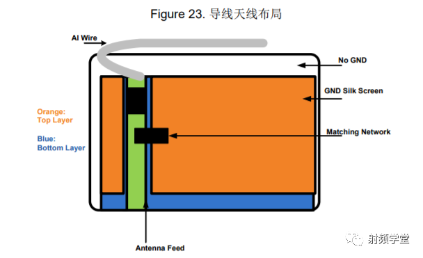
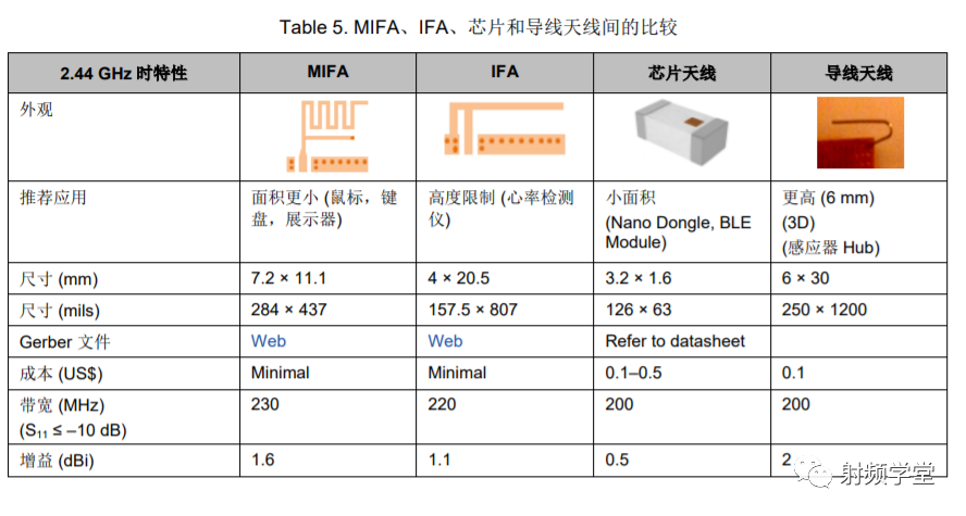
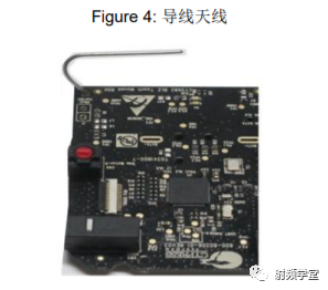
1. Wire Antenna: This is a segment of wire extended into free space on the PCB, with a length of Lambda/4, placed on a ground plane. This type of antenna is powered by a 50-Ω impedance transmission line. Generally, due to size and exposure in three dimensions, the performance and radiation range provided by this wire antenna is the best. The wire can be straight, helical, or looped. It is a three-dimensional (3D) structure, where the antenna rises 4-5mm above the PCB and extends into space.
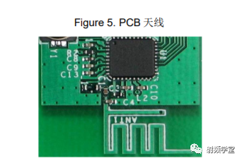
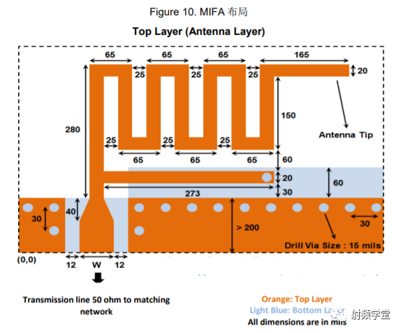
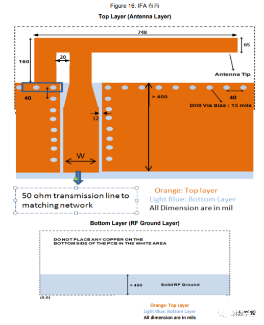
 2. PCB Antenna: This is a trace on the PCB that can be drawn in a straight line, inverted-F shape, serpentine, or circular trace, or based on the antenna type and spatial constraints, a swinging curve, etc. In a PCB antenna, the antenna becomes a two-dimensional (2D) structure on the same plane as the PCB; see Figure 5. When a 3D antenna exposed to space is placed on the PCB layer as a 2D trace, certain guidelines must be followed. Generally, it requires more PCB space than a wire antenna, has lower efficiency, but is cheaper, easier to manufacture, and can provide acceptable wireless distance for BLE applications.
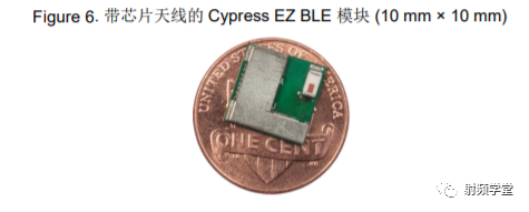
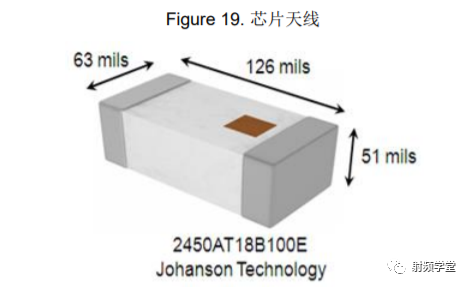
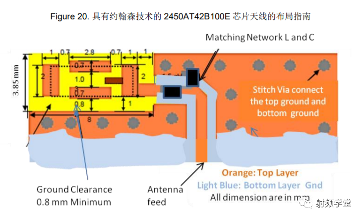
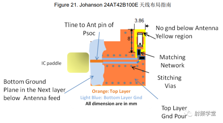
3. Chip Antenna: This is an antenna with conductors that are assembled within a small IC package. This is very useful when space for printed PCB antennas is limited or when supporting 3D wire antennas. See Figure 6 for a Bluetooth module containing a chip antenna. Below is a comparison of the size of the antenna and module with a one-cent coin.
The selection of antennas depends on factors such as their application, the size of the available circuit board, cost, radiation range, and directionality. Bluetooth Low Energy (BLE) applications (like wireless mice) only require a radiation range of 10 feet and a few kbps data rate. However, for remote control applications using voice recognition, an indoor antenna setup is required, with a radiation range of about 20 feet and a data rate of 64 kbps.
The following section provides some key parameters for antenna performance.
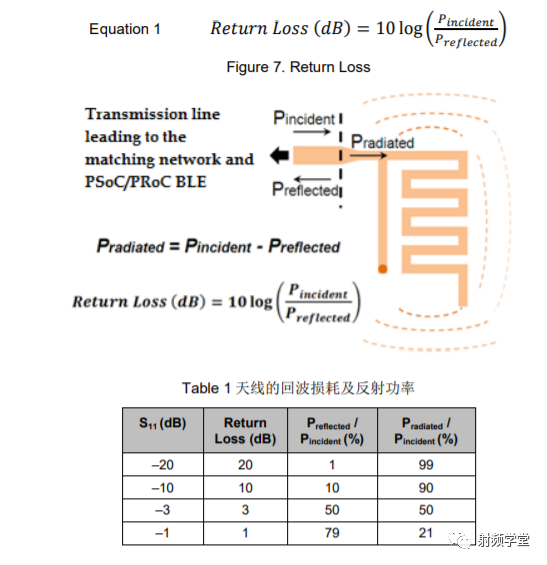
▪ Return Loss: The return loss of an antenna indicates how the antenna matches with a transmission line (TL) of 50 Ω impedance, as shown in the signal feed in Figure 7. Typically, this TL has an impedance of 50 Ω, but it can also be other values. For industrial standards, commercial antennas and their testing equipment resistances are 50 Ω, so it is recommended to use this value. Return loss shows the magnitude of the incident power reflected by the antenna due to mismatch (Formula 1). An ideal antenna would radiate all power without any reflection. If the return loss is infinite, the antenna is considered perfectly matched to the TL, as shown in Figure 7. S11 is the reciprocal of return loss, measured in dB. In most cases, if return loss ≥ 10 dB (i.e., S11 ≤ -10 dB), it is sufficiently large. Table 1 shows the return loss (dB) of the antenna and the reflected power (%). A return loss of 10 dB indicates that 90% of the incident power is transferred to the antenna for transmission.
2. PCB Antenna: This is a trace on the PCB that can be drawn in a straight line, inverted-F shape, serpentine, or circular trace, or based on the antenna type and spatial constraints, a swinging curve, etc. In a PCB antenna, the antenna becomes a two-dimensional (2D) structure on the same plane as the PCB; see Figure 5. When a 3D antenna exposed to space is placed on the PCB layer as a 2D trace, certain guidelines must be followed. Generally, it requires more PCB space than a wire antenna, has lower efficiency, but is cheaper, easier to manufacture, and can provide acceptable wireless distance for BLE applications.
3. Chip Antenna: This is an antenna with conductors that are assembled within a small IC package. This is very useful when space for printed PCB antennas is limited or when supporting 3D wire antennas. See Figure 6 for a Bluetooth module containing a chip antenna. Below is a comparison of the size of the antenna and module with a one-cent coin.
The selection of antennas depends on factors such as their application, the size of the available circuit board, cost, radiation range, and directionality. Bluetooth Low Energy (BLE) applications (like wireless mice) only require a radiation range of 10 feet and a few kbps data rate. However, for remote control applications using voice recognition, an indoor antenna setup is required, with a radiation range of about 20 feet and a data rate of 64 kbps.
The following section provides some key parameters for antenna performance.
▪ Return Loss: The return loss of an antenna indicates how the antenna matches with a transmission line (TL) of 50 Ω impedance, as shown in the signal feed in Figure 7. Typically, this TL has an impedance of 50 Ω, but it can also be other values. For industrial standards, commercial antennas and their testing equipment resistances are 50 Ω, so it is recommended to use this value. Return loss shows the magnitude of the incident power reflected by the antenna due to mismatch (Formula 1). An ideal antenna would radiate all power without any reflection. If the return loss is infinite, the antenna is considered perfectly matched to the TL, as shown in Figure 7. S11 is the reciprocal of return loss, measured in dB. In most cases, if return loss ≥ 10 dB (i.e., S11 ≤ -10 dB), it is sufficiently large. Table 1 shows the return loss (dB) of the antenna and the reflected power (%). A return loss of 10 dB indicates that 90% of the incident power is transferred to the antenna for transmission.
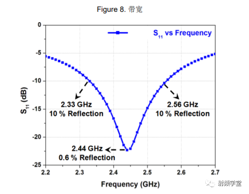
 ▪ Bandwidth: This refers to the frequency response of the antenna. It indicates how the antenna matches with the 50 Ω transmission line across the entire band used, specifically in the range of 2.40 GHz to 2.48 GHz for BLE applications.
As shown in Figure 8, the return loss is greater than 10 dB in the bandwidth from 2.33 GHz to 2.55 GHz. Therefore, the bandwidth used is about 200 MHz. In most cases, a wider bandwidth is preferred as it minimizes the detuning effects caused by environmental changes around the antenna during actual use (e.g., a mouse placed on wood/metal/plastic tables, with hands around the mouse, etc.).
▪ Radiation Efficiency: This refers to the portion of non-reflected power (see Figure 7) that is consumed as heat in the antenna. Heat generation is due to dielectric losses in the FR4 substrate and conductor losses in the copper wire. This information is referred to as radiation efficiency. When the radiation efficiency is 100%, all non-reflected power is radiated into space. For small PCB form factors, thermal losses are minimal.
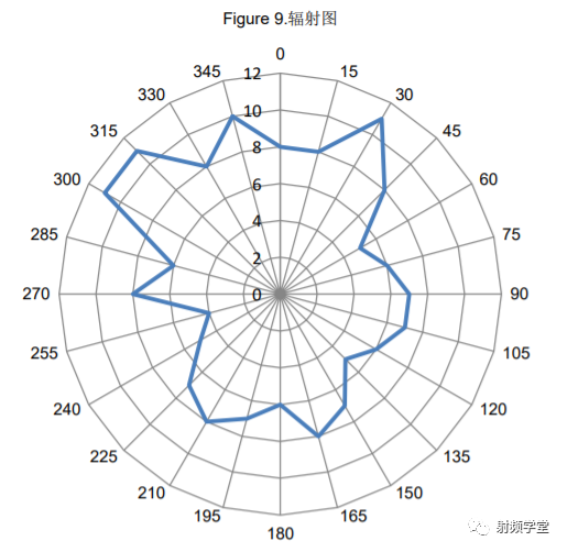
▪ Radiation Pattern: This pattern represents the directionality of radiation, indicating in which direction radiation is stronger and in which direction it is weaker. It helps accurately determine the direction of the antenna in applications.
Omnidirectional antennas can equivalently emit in all directions on a plane perpendicular to the axis. However, most antennas do not achieve this ideal performance. For detailed explanations, please refer to the radiation pattern of the PCB antenna shown in Figure 9. Each data point represents the RF field strength, which can be measured by the indicator (RSSI) used in the receiver for signal strength. As expected, the resulting profile is not circular because the antenna is not isotropic.
▪ Gain: Gain provides information on the radiation in the adopted direction compared to an isotropic antenna (which can emit from all directions). The unit of gain is “dBi,” indicating the field strength of radiation compared to an ideal isotropic antenna.
Antenna Introduction Diagram
Comparison of Various Antennas
Antenna Placement, Housing, and Ground Plane Guidelines
▪ Always place the antenna at a corner of the PCB, maintaining sufficient clearance from the rest of the circuit.
▪ Always follow the grounding method recommended by the antenna designer/manufacturer. Common PCB antennas are variations of monopole antennas. Monopole antennas require direct grounding to function properly.
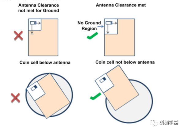
▪ Never place any components, planes, mounting screws, or traces in the antenna exclusion zone on all layers. The actual exclusion zone depends on the antenna used.
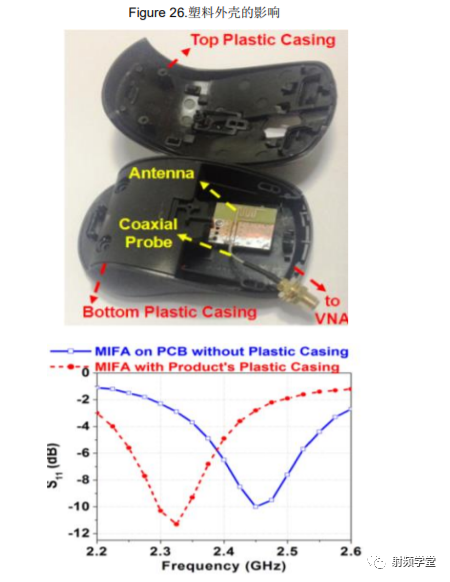
▪ Do not place the antenna close to plastics in industrial designs. Plastics have a higher dielectric constant than air. Proximity of plastic to the antenna causes the antenna to see a higher effective dielectric constant. This increases the electrical length of the antenna trace and lowers the resonant frequency.
▪ Battery cables or microphone cables must not cross the antenna trace.
▪ The antenna must not be completely covered by a metal housing. If the product has a metal housing or shielding, the housing must not cover the antenna. No metal is allowed in the near field of the antenna.
▪ The orientation of the antenna should be consistent with the final product orientation to maximize radiation in the desired direction.
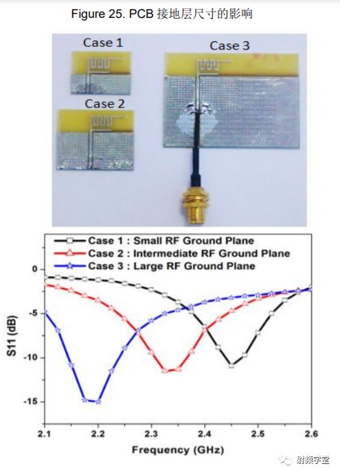
▪ There should be no ground beneath the antenna.
▪ There should be sufficient space (clearance) from the antenna to the ground plane, and the width of that ground plane should be minimal.
▪ Plan for configurations for the antenna matching network, as many parameters affecting the antenna (plastics, ground variations, substrate differences, and other components) may change its impedance, necessitating retuning of the antenna. If the impedance of the antenna is unknown, it is best to provide configurations for a PI or T network of three components, with series elements filled with 0 ohms and shunt elements unloaded. This helps you later fill in any topology required for the matching network.
▪ When using matching network values provided by the antenna manufacturer, ensure to use the trace length from the antenna to the matching network specified in the manufacturer’s data sheet or reference design.
▪ Always verify the antenna matching network using the final plastic housing and typical usage scenarios, such as verifying a mouse’s plastic when held in hand, placed on a mouse pad, plastic, wood, metal, or floor.
In addition to the introduction of antennas, this guide also covers the basics of RF knowledge in detail. Students who need the full text can leave a message at the end. Thank you.
▪ Bandwidth: This refers to the frequency response of the antenna. It indicates how the antenna matches with the 50 Ω transmission line across the entire band used, specifically in the range of 2.40 GHz to 2.48 GHz for BLE applications.
As shown in Figure 8, the return loss is greater than 10 dB in the bandwidth from 2.33 GHz to 2.55 GHz. Therefore, the bandwidth used is about 200 MHz. In most cases, a wider bandwidth is preferred as it minimizes the detuning effects caused by environmental changes around the antenna during actual use (e.g., a mouse placed on wood/metal/plastic tables, with hands around the mouse, etc.).
▪ Radiation Efficiency: This refers to the portion of non-reflected power (see Figure 7) that is consumed as heat in the antenna. Heat generation is due to dielectric losses in the FR4 substrate and conductor losses in the copper wire. This information is referred to as radiation efficiency. When the radiation efficiency is 100%, all non-reflected power is radiated into space. For small PCB form factors, thermal losses are minimal.
▪ Radiation Pattern: This pattern represents the directionality of radiation, indicating in which direction radiation is stronger and in which direction it is weaker. It helps accurately determine the direction of the antenna in applications.
Omnidirectional antennas can equivalently emit in all directions on a plane perpendicular to the axis. However, most antennas do not achieve this ideal performance. For detailed explanations, please refer to the radiation pattern of the PCB antenna shown in Figure 9. Each data point represents the RF field strength, which can be measured by the indicator (RSSI) used in the receiver for signal strength. As expected, the resulting profile is not circular because the antenna is not isotropic.
▪ Gain: Gain provides information on the radiation in the adopted direction compared to an isotropic antenna (which can emit from all directions). The unit of gain is “dBi,” indicating the field strength of radiation compared to an ideal isotropic antenna.
Antenna Introduction Diagram
Comparison of Various Antennas
Antenna Placement, Housing, and Ground Plane Guidelines
▪ Always place the antenna at a corner of the PCB, maintaining sufficient clearance from the rest of the circuit.
▪ Always follow the grounding method recommended by the antenna designer/manufacturer. Common PCB antennas are variations of monopole antennas. Monopole antennas require direct grounding to function properly.
▪ Never place any components, planes, mounting screws, or traces in the antenna exclusion zone on all layers. The actual exclusion zone depends on the antenna used.
▪ Do not place the antenna close to plastics in industrial designs. Plastics have a higher dielectric constant than air. Proximity of plastic to the antenna causes the antenna to see a higher effective dielectric constant. This increases the electrical length of the antenna trace and lowers the resonant frequency.
▪ Battery cables or microphone cables must not cross the antenna trace.
▪ The antenna must not be completely covered by a metal housing. If the product has a metal housing or shielding, the housing must not cover the antenna. No metal is allowed in the near field of the antenna.
▪ The orientation of the antenna should be consistent with the final product orientation to maximize radiation in the desired direction.
▪ There should be no ground beneath the antenna.
▪ There should be sufficient space (clearance) from the antenna to the ground plane, and the width of that ground plane should be minimal.
▪ Plan for configurations for the antenna matching network, as many parameters affecting the antenna (plastics, ground variations, substrate differences, and other components) may change its impedance, necessitating retuning of the antenna. If the impedance of the antenna is unknown, it is best to provide configurations for a PI or T network of three components, with series elements filled with 0 ohms and shunt elements unloaded. This helps you later fill in any topology required for the matching network.
▪ When using matching network values provided by the antenna manufacturer, ensure to use the trace length from the antenna to the matching network specified in the manufacturer’s data sheet or reference design.
▪ Always verify the antenna matching network using the final plastic housing and typical usage scenarios, such as verifying a mouse’s plastic when held in hand, placed on a mouse pad, plastic, wood, metal, or floor.
In addition to the introduction of antennas, this guide also covers the basics of RF knowledge in detail. Students who need the full text can leave a message at the end. Thank you.
Previous Recommendations, Click to View
Huawei: Introduction to Antenna Basics
What is the relationship between the number of oscillators, antennas, channels, and streams in 5G MM?
How to design multi-frequency antennas for mobile phones?
Is the design of 5G terminal antennas difficult?
Simulation design of 5G mobile phone antennas
Practical design notes for mobile phone antennas
Microstrip patch antenna simulation design, So Easy!
This classic antenna work is still worth recommending today
How to simulate antennas with HFSS scripts?
Fundamentals of microstrip antenna design (with download)
PPT: Introduction to Antenna Basics
Huawei: Introduction to Antenna Basics
A detailed explanation of base station antennas
Note: 【RF Academy】 reprints, all articles are owned by the original author, sharing is for learning purposes. If there are any objections, please contact RF Academy to delete or modify. We wish you much learning and many gains at RF Academy!
[RF Resources Download][Essential RF Basics][Must-Read Exciting Articles]
👆Join Group/Recruitment/Reprint/Cooperation/Submission/Promotion, Find RF Carpenter👆
👇Scan the QR code for more exciting content👇