Welcome FPGA engineers to join the official WeChat technical group.
Clickthe blue textto follow us at FPGA Home – the largest pure FPGA engineer community in China.

FPGAs, Zynq, and Zynq MPSoC!
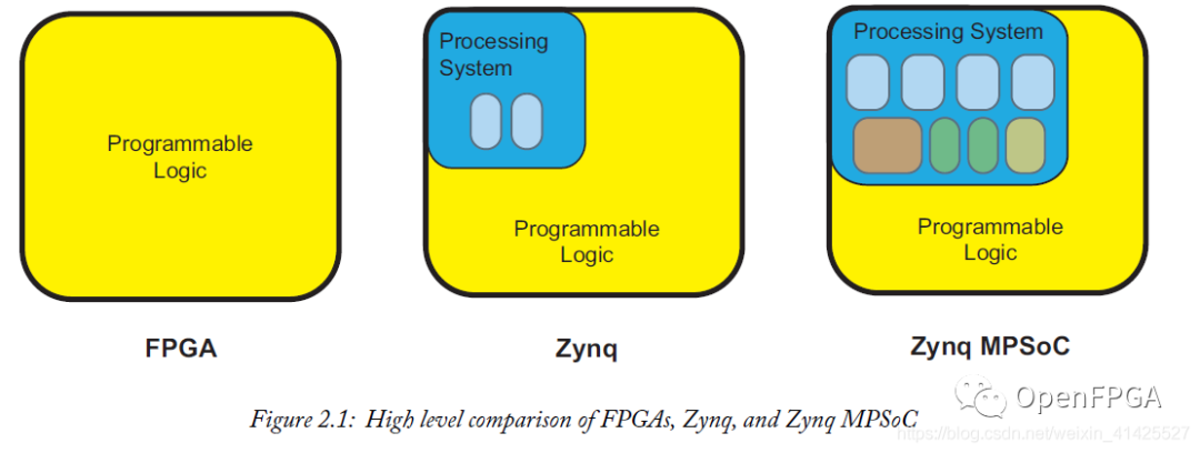
Zynq MPSoC is an evolved version of the Zynq-7000 SoC (hereafter referred to as Zynq). Zynq is the first generation of integrated PL (FPGA) and PS design products released by Xilinx. As shown in Figure 2.1, a comparative analysis of the three devices is presented at a relatively high level. The PS part of the Zynq MPSoC is larger and more complex than that of Zynq. This chapter will introduce the characteristics of these three devices.
2.1 Technology Timeline
Before further introduction, it should be noted that each of these three products has its own advantages. When choosing, it is not the case that more expensive is better, but rather that the most suitable choice for our design is the best choice. All three products have their own best balance in terms of cost and performance, making them suitable for different tasks and applications.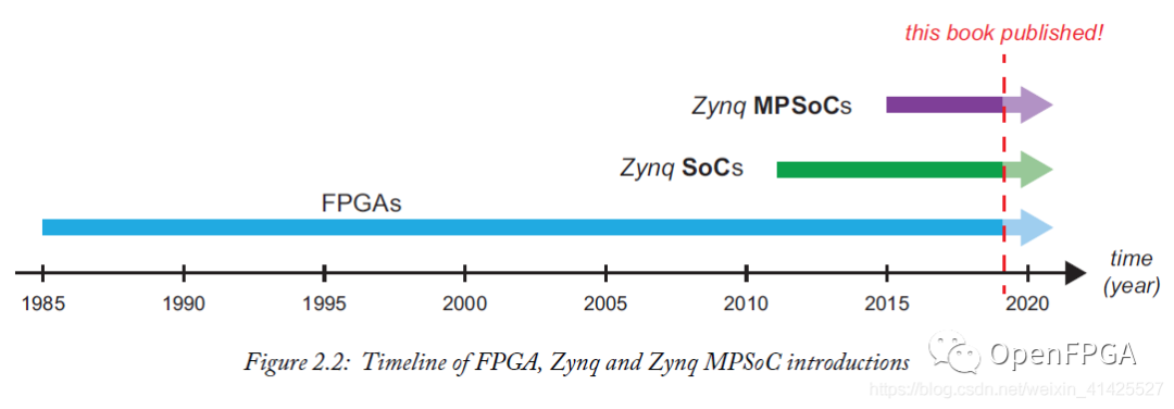 Since most readers are more familiar with Zynq, we will start with it for easier comparison with Zynq MPSoC later. Since FPGA is the PL part of all SoC products, we will introduce it later.
2.2 Zynq-7000 SoC
Zynq-7000 SoC is the first SoC device released by Xilinx. It integrates the FPGA-based PL part and the Arm-based PS part. Here, we will provide a brief introduction. For more detailed information, please refer to [The Zynq Book] (http://www.zynqbook.com/), which has been published in Chinese.
2.2.1 Zynq Architecture Features
From a high-level perspective, the Zynq architecture consists of PS and PL parts and the interconnects between them. As shown in Figure 2.3, the interconnection follows the AXI standard, which is a chip communication technology standard developed by Arm.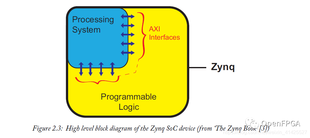 Integrating PS and PL together provides dedicated optimized resources for running the software-based parts of embedded systems (my understanding is that it is suitable for parts running on processors) and leverages the advantages of FPGA (especially its parallelism and configurability). The AXI interface connects these two parts, optimized specifically for SoC applications. The sizes in Figure 2.3 are not drawn to scale; different Zynq devices have the same PS architecture, but different sizes of PL parts. For Zynq and Zynq MPSoC, their PS and PL parts are different.
Zynq PS Part
The blue part in Figure 2.3 is an application-level processor and related components, as follows:
-
Application Processor Unit (APU) – This part includes a dual-core Arm Cortex-A9 processor and 256KB of on-chip cache.
-
Interconnect and Storage Interface – Used for PL and PS communication as well as communication with their respective external storage units.
-
I/O Peripherals – A range of integrated peripheral interfaces, including common standards such as USB, UART, SPI, I2C, etc.
The PS part of Zynq contains two processing cores, allowing designers to run the same operating system on both cores or run different operating systems on each core. Later, we will compare the PS architecture of Zynq and Zynq MPSoC and explain some additional features introduced in the new device. In fact, Zynq MPSoC has six processing cores.
Recently (around 2019), a lightweight version of Zynq, Zynq-7000S, was released, which includes only one Cortex-A9 processor in its PS.
Zynq PL Part
The PL part of Zynq is based on Xilinx’s FPGA devices, and its performance corresponds to the PL performance, including Xilinx’s Artix-7, Kintex-7, and Virtex-7 series devices. Like these FPGAs, its PL part includes DSP48x slices (high-speed computing resources), Block RAMs, high-speed transceivers, integrated communication modules, and general logic. Section 2.4.3 will further introduce these modules of modern FPGAs.
Zynq PS and PL Interface
The PL and PS parts of Zynq have nine interfaces, including four “general-purpose interfaces”, four “high-performance” interfaces, and one “accelerated consistency” interface for communication between the APU in PS and PL.
2.2.2 Zynq Devices
Table 2.1 compares the key features and parameters of the Zynq-7000 series devices (note that the single-core Zynq-7000S series is not included in this comparison; see the Zynq-7000 SoC Data Sheet: Overview document). For the listed Zynq-7000 series devices, there is no difference in the PS part except for the maximum supported clock frequency. The PL part is similar to the FPGA model it is based on, e.g., the PL part based on Artix-7 is similar to Artix-7 resources. Different models of the PL part differ in DSP slices, Block RAM, and input/output resources.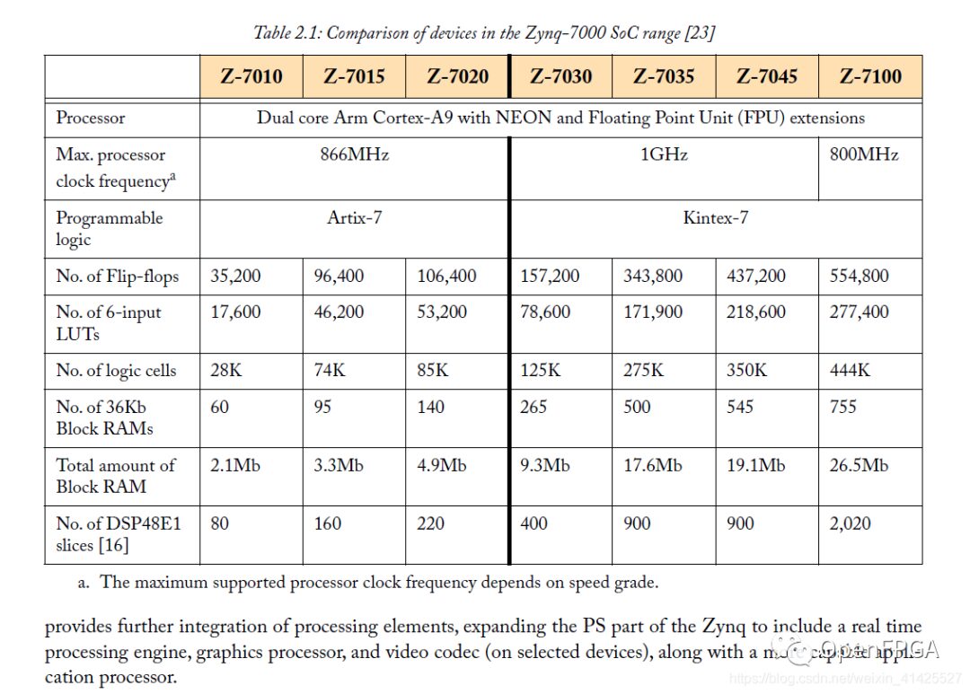
2.3 Xilinx Zynq MPSoC
Zynq MPSoC is an advanced version of Zynq, with a more complex PS part, and the PL part upgraded from the Xilinx 7 series to UltraScale+ FPGA architecture. For most Zynq MPSoC devices, the resources and area of the PL part are greater than those of the Zynq series.
2.3.1 Zynq MPSoC Release
Zynq MPSoC was released in 2015, four years after the release of Zynq. During these four years, Zynq was applied in many fields, leading to the demand for “FPGA + processor”. Zynq MPSoC provides an enhanced PS and more resources and area in PL, containing different sub-series to meet various application needs. The different sub-series are represented by two uppercase letters, namely CG series, EG series, and EV series, as shown in Table 2.2. Zynq MPSoC is not a replacement for Zynq; it provides an extended enhanced solution in the same form. Zynq is more suitable for relatively low-power and slightly simpler systems.
2.3.2 Zynq MPSoC Architecture and Features
The resources of the PS and PL parts of the three sub-series of Zynq MPSoC are shown in Table 2.4; these features will be detailed in the following chapters of this book.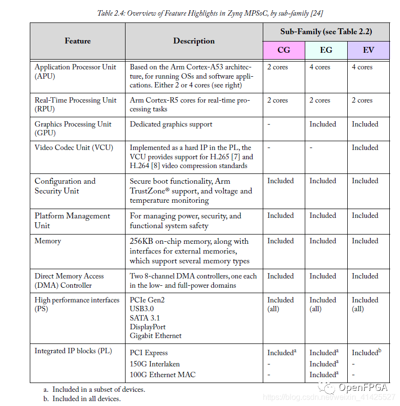 Another important feature of the Zynq MPSoC architecture is its power management capabilities. The device is divided into four power domains that can be controlled individually, allowing power to be cut off (power down) to idle parts, improving power efficiency. In addition, the security aspects of the Zynq MPSoC architecture have also been further strengthened. It is worth emphasizing that the UltraScale+ FPGA architecture (discussed in section 2.4.3) used in the PL part of the Zynq MPSoC has significant enhancements compared to the 7 series used in Zynq. Two very important features are that it includes UltraRAM and that the DSP has evolved from DSP48E1 to DSP48E2. The resources of the PL parts of this device series vary by model, and Table 2.3 presents the minimum and maximum resources available. Compared to the PL part of Zynq (Table 2.1), Zynq MPSoC has more resources, suitable for developing applications that require higher PL resources.

2.4 FPGA
FPGA is the foundation of the PL parts of the above two devices and is also the earliest device to appear. Therefore, we will review its development, followed by an introduction to some applications, and finally discuss the architecture and features of modern FPGA technology.
2.4.1 What is FPGA
(There is a lot of information about FPGA, so we will not elaborate on it here.)
2.4.2 FPGA Development
Xilinx’s FPGA architecture started with only 64 flip-flops and 3-input lookup tables (LUTs to implement logic functions). With the development of FPGA technology, its area has continuously increased, and logic resources have expanded. Its architecture has also evolved, with power consumption steadily decreasing, allowing for higher frequencies. Additionally, a large number of dedicated resources such as high-speed memory, computing modules, clocks, and interconnects continue to develop. From the perspective of FPGA scale, measuring logic density using “logic cells”, we consider the differences in architecture at a slightly abstract lower level. Figure 2.4 summarizes the development of FPGAs in terms of “logic cells” over a timeline of 15 years, with 5-year intervals. Comparing it to the first FPGA (released in 1985), it can be seen that modern FPGAs have grown significantly even compared to the developments of the last decade, let alone earlier FPGAs. The first FPGA can only be represented as a point on the left side of the figure. Additionally, this year, there are also some relatively low-end devices available for developers with less demanding needs. The small boxes within the larger box represent the lower-end devices of that series.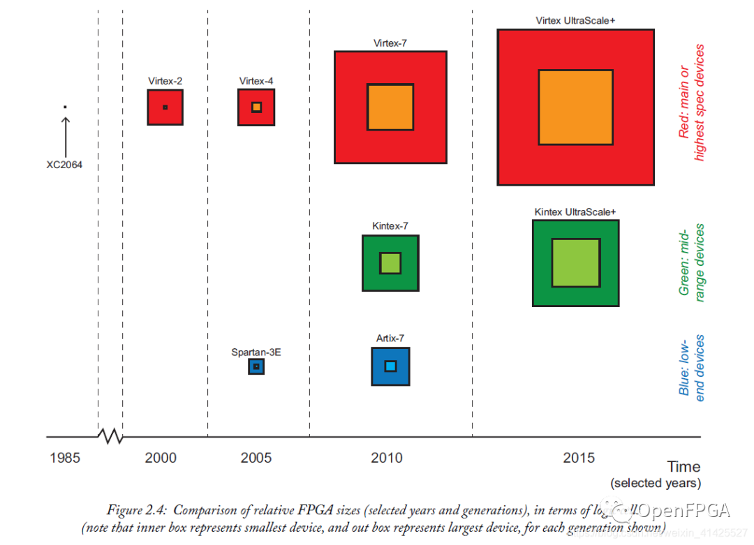 Comparing only the logic cells, Table 2.5 provides a comparison between XC2064 and the most advanced device, Virtex UltraScale+ VU13P. This does not include the advancements in architecture and other advanced features that have been developed in recent years.
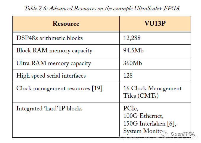 Xilinx’s basic FPGA structure remains a two-dimensional array of digital logic elements grouped into CLBs. Each CLB contains a small number of flip-flops and lookup tables, where LUTs are used to implement Boolean logic functions, small memory blocks, and shift registers. At a lower level, the composition of CLBs has evolved over time, with modern CLBs containing more logic resources than earlier CLBs. We have retained this term; CLB is still the connection of programmable interconnects and switch matrices. Of course, this connection technology has also significantly improved. In Figure 2.5, a diagram of the array structure of CLBs can be seen, with switch matrices and programmable interconnects visible at the bottom of the figure. With the development of application requirements, FPGA architecture continues to evolve, with larger memory units (from Block RAM to the recent Ultra RAM) providing higher density and speed storage capabilities, such as enabling the storage of video data within the device. Around 2000, multipliers were integrated, followed by the integration of arithmetic processing modules (DSP48x slices) capable of performing multiplication, addition, and other logical computations. Certainly, DSP has also undergone significant development over the years. As FPGA technology is increasingly applied in fundamental communication infrastructure, data centers, and high-performance cloud computing, the value of IP blocks supporting high-speed serial interfaces has grown significantly. As shown in Table 2.6, in addition to larger areas, the latest FPGAs contain more specialized resources and functionalities.
 In the next section, we will continue to discuss more details of UltraScale+ FPGAs.
Modern FPGA Architecture: UltraScale+
The modern FPGA architecture is essentially a two-dimensional array of the device. In some sense, it is similar to earlier devices. Its features, as previously emphasized, include richer resources and larger device areas. Figure 2.5 illustrates the resources of UltraScale+ FPGAs; from a higher abstract level, this figure can be considered as composed of blocks arranged vertically. Most areas belong to general-purpose logic (general purpose logic), such as CLBs composed of lookup tables and flip-flops. Another portion of the area consists of Ultra RAM memory blocks and DSP58x computing units, arranged in single or double columns, forming narrow vertical striped areas. In terms of interfaces, input/output blocks are arranged in banks and form columns in the main resource array. Input/output blocks (IOB) support various interface standards. Additional connections are provided in the form of high-speed serial transceivers, which are usually located in four groups at the edges of the FPGA. Based on these, dedicated blocks are provided to support selected communication standards (see Table 2.6). Additional resources for configuration, clock management, and system monitoring are also present in the FPGA architecture.
DSP Functions
Most operations in digital signal processing (DSP) are fixed-point multiplication and addition operations. Common DSP tasks, such as Finite Impulse Response (FIR) filtering and Fast Fourier Transform (FFT) computations, primarily involve addition/subtraction, multiplication, and sample delays. In Xilinx FPGAs, these operations are mainly performed by DSP48x slices. The simplified block diagram of this slice is shown in Figure 2.6, which displays its algorithm operations and word lengths, omitting some additional features such as delay elements, signal paths, and multiplexers. To implement FIR or FFT, DSP48E2 slices can be cascaded together (without consuming FPGA resources). For example, to implement an adder longer than the word length of a single DSP slice—say a 96-bit adder—multiple DSP48E2 slices can be combined. In addition to computational functionality, DSP48E2 slices can also be used for barrel shift registers, pattern detection, and other logical operations. For more complete information about DSP48E2, including details of improvements compared to previous DSP48Ex, please refer to the document: UltraScale Architecture DSP Slice: User Guide.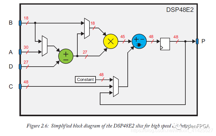
Storage Support
Memory in FPGAs can consist of CLB resources, and memory resources formed by CLBs are often used to store small amounts of data. For larger storage, Block RAM (which can store 36Kb or be divided into two 18Kb memories) can be used. In UltraScale devices, Ultra RAM (288Kb each) with greater storage capacity is integrated. Larger memory can be achieved by combining Block RAM or Ultra RAM. Block RAM and Ultra RAM are implemented as dedicated physical blocks on the FPGA, rather than being composed of general lower-level logic elements. They support high-performance operations and can operate at the maximum clock frequency supported by the device. Ultra RAM can be powered down individually when not in use. For more details on Ultra RAM, please refer to the document: UltraRAM: Breakthrough Embedded Memory Integration on UltraScale+ Devices. Figure 2.7 shows the four types of available memory resources on the FPGA.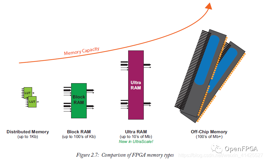 As the device area increases, especially with the introduction of Ultra RAM, on-chip storage capacity continues to enhance, reducing or even eliminating dependence on off-chip storage. This minimizes additional system consumption, interface efforts, energy consumption, as well as latency and performance limitations. Each type of storage in Figure 2.7 has its own characteristics, allowing for suitable choices in different tasks. Depending on the design approach taken, designers can choose specific storage resources or let synthesis tools select them directly.
2.5 Comparison and Discussion: FPGA, Zynq, and Zynq MPSoC
This section summarizes the different characteristics of FPGA, Zynq, and Zynq MPSoC, including their architectures, power consumption, performance, and characteristics in embedded system implementations.
2.5.1 Architecture
(Most of the content in this subsection has been mentioned previously; here we provide a conclusive table, and for more detailed summaries, please refer to the original book.)
2.5.2 Power Consumption and Performance
Over the years, power consumption has been reduced while performance (i.e., maximum processing frequency or “speed”) has improved. From the Xilinx FPGA released in 1985 to the 7 series devices released in 2011, energy consumption (measured per logic unit) has decreased by more than 1000 times. At the same time, performance has increased by about 100 times. Below we provide a simple comparison of these devices.
Power Consumption
(Refer to the original book)
Performance
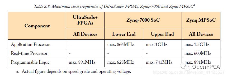
Computational performance is typically measured by maximum processing frequency. To compare performance, Table 2.8 compares the maximum clock frequencies of PS and PL components. In summary, the power consumption of FPGA and SoC devices is closely related, as all SoCs include a PL area that is effectively the same as that of FPGAs. Compared to Zynq and Zynq MPSoC, the power consumption (per logic unit) of Zynq MPSoC devices is lower, and overall performance is higher, due to various optimizations of the UltraScale+ FPGA architecture. In terms of PS, the Zynq MPSoC architecture is more complex, offering higher performance and additional features such as power management.
2.5.3 Embedded System Implementation
(Refer to the original book)
2.5.4 Applications
(Refer to the original book)
2.6 Conclusion
(Refer to the original book)
References: L. H. Crockett, D. Northcote, C. Ramsay, F. D. Robinson and R. W. Stewart, Exploring Zynq MPSoC: With PYNQ and Machine Learning Applications, First Edition, Strathclyde Academic Media, 2019. Original link: https://www.zynq-mpsoc-book.com/wp-content/uploads/2019/04/MPSoC_ebook_web_v1.0.pdf
(You can jump to read the original text)
Source: https://www.zynq-mpsoc-book.com/wp-content/uploads/2019/04/MPSoC_ebook_web_v1.0.pdf
Copyright belongs to the original author.

Welcome FPGA, embedded, signal processing engineers to follow our official account.

The largest FPGA WeChat technical group in the country
Everyone is welcome to join the national FPGA WeChat technical group, which has tens of thousands of engineers, a group of engineers who love technology, where FPGA engineers help each other and share knowledge, creating a strong technical atmosphere!Hurry up and invite your friends to join!!

Press and hold to join the national FPGA technical group.
FPGA Home Component City
Advantageous component services, please scan the code to contact the group owner: Jin Juan Email: [email protected] Welcome to recommend to procurement.
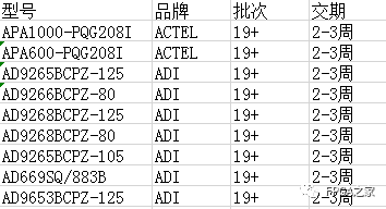
Advantageous orders for ACTEL, AD (full series):
Advantageous stock or orders for XILINX, ALTERA (full series):
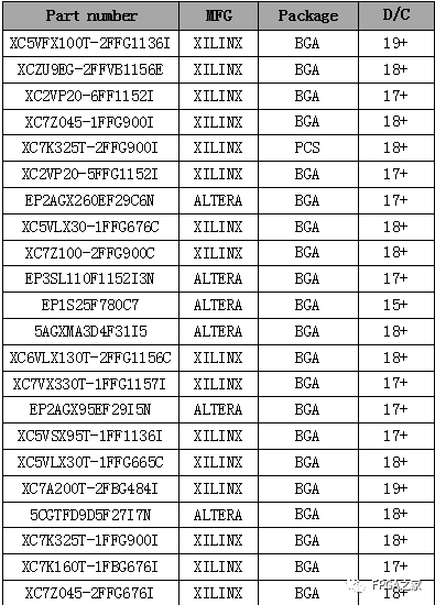
(The above components are part of the models; for more models, please consult group owner Jin Juan.)
Service philosophy: FPGA Home Components self-operated City aims to facilitate engineers in quickly and conveniently purchasing components. After years of dedicated service, our customer service covers large listed companies, military research units, and small and medium enterprises. Our biggest advantage is emphasizing service first, and achieving fast delivery and favorable prices!
Directly operated brands: Xilinx, ALTERA, ADI, TI, NXP, ST, E2V, Micron, and over a hundred other component brands, especially adept at dealing with components under the US embargo against China.We welcome engineering friends to recommend us to procurement or consult us directly!We will continue to provide the best service in the industry!

Official thanks to brands in the FPGA technical group: Xilinx, Intel (Altera), Microsemi (Actel), Lattice, Vantis, Quicklogic, Lucent, etc.