Chip mounting is a core process in semiconductor packaging, and the choice of technology directly affects the thermal management, electrical performance, and long-term reliability of devices. This article systematically analyzes the process characteristics and applicable scenarios of four mainstream mounting technologies and discusses industry development trends.
For more common topics, click above to follow and set as a star!
1. Eutectic Bonding Technology
1. Technical Principle
Based on the metal eutectic reaction (such as the Au-Si system), when the temperature reaches the eutectic point (363°C for the Au-Si system), the two metals form a liquid alloy, which solidifies into a high-strength metallurgical bond upon cooling. The key to this technology lies in the precise control of the temperature curve and atmospheric environment (usually using nitrogen protection).
2. Process Innovation
Modern processes utilize laser-assisted heating and ultrasonic vibration technology, reducing the process time to the millisecond level. For example, using pulsed lasers can create a localized liquid phase, combined with ultrasonic vibration to eliminate micro-voids, achieving a bonding strength of over 30 MPa.
2. Solder Mounting Technology
1. Evolution of Material Systems
Hard solders (Au-Ge, Au-Sn) are evolving towards lower temperatures, with new Sn-Ag-Cu (SAC) alloys having melting points as low as 217°C. Soft solders based on Pb have gradually been replaced by lead-free alternatives, such as In-Bi alloys (melting point 79°C).
2. Stress Control Technology
By designing stress buffer layers (such as porous copper pillar structures) and gradient materials, thermal mismatch stress can be reduced by 60%. The micro-bump technology used in 3D packaging has reduced the diameter to the 10 μm level, with a pitch of 20 μm.
3. Conductive Adhesive Mounting Technology
1. Material Breakthrough
Nano-silver conductive adhesives (particle size <50nm) have achieved a resistivity as low as 10^-5 Ω·cm, approaching metal levels. Anisotropic conductive adhesives (ACF) have achieved 5 μm pitch connections in display driver chip packaging.
2. Reliability Improvement
Composite conductive adhesives with added silica nanoparticles have improved shear strength retention by 80% at 150°C. UV-curable conductive adhesives can reduce process time to the second level.
4. Glass Adhesive Mounting Technology
1. High-Temperature Packaging Solutions
Low-temperature glass systems (softening point <400°C) combined with silver-copper alloys achieve a thermal conductivity of 80 W/mK. Gradient sintering processes can achieve reliable connections between ceramic substrates and silicon chips, withstanding 1000 cycles of -55~150°C thermal cycling.
2. Micro-Electro-Mechanical Systems (MEMS) Applications
Photo-sensitive glass adhesives achieve patterned bonding with a thickness of 50 μm, with airtightness reaching 10^-8 Pa·m³/s, meeting the packaging requirements for inertial sensors.
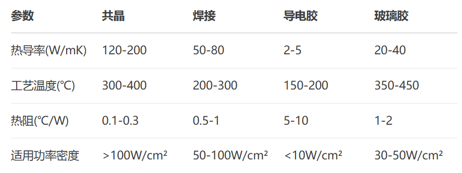
5. Technology Comparison and Development Trends
Table 1: Comparison of Mounting Technology Performance
Future Development Directions:
1. Hybrid Mounting Technology: Eutectic + conductive adhesive composite structures for gradient thermal management.
2. Nano Bonding: Room temperature mounting technology based on metal nanowires.
3. Smart Materials: Shape memory alloys for self-regulating stress structures.
4. Heterogeneous Integration: Hybrid bonding technology in 3D stacking.
With the development of 5G, artificial intelligence, and power electronics, chip mounting technology is advancing towards ultra-precision, high reliability, and multifunctionality. The synergistic progress of material innovation and process reform will continue to drive packaging technology beyond physical limits, providing critical support for the next generation of electronic devices.
Like + View
Share with your friends! ↓