13.2
Analysis of CGC Clock Configuration Block Diagram
Opening the clock configuration page in the #FSP configurator, the default clock configurations for the RA6M5/RA4M2/RA2L1 without modifications are shown in the three images below. These #clock configuration diagrams are primarily designed to facilitate user configuration, and their structure is relatively simple, resembling a simplified version of the clock tree. For a complete clock tree, readers are referred to Chapter 8 “Clock Generation Circuit” of the corresponding RA chip hardware manual, which is more complex and not suitable for direct analysis in this context. Interested readers can refer to the complete clock tree in the manual while reading this section.
In the following three clock configuration diagrams, we can see that the actual flow of clock signal generation in the FSP clock configuration page follows the darker black arrows. The lighter gray arrows indicate clock routes that are not actually used; at the hardware level, this part of the circuit will not be configured or enabled.
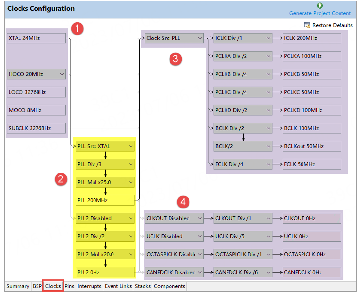
The default clock configuration for the RA6M5 in the FSP configurator is shown in the image below:
Click to view the full image
In the above image, following the direction of the solid black arrows, XTAL is the external high-speed crystal oscillator, also known as MOSC. By examining the schematic of the Qiming 6M5 development board, we can see that it is connected to an external crystal oscillator with a frequency of 24MHz, so this setting is correct and does not require modification. Continuing down, in the PLL clock source selection (PLLSrc), the external high-speed crystal oscillator (XTAL) is chosen as the PLL clock source. The PLL then divides by 3 and multiplies by 25, resulting in an output clock frequency of 200MHz: 24MHz/3*25=200MHz. Continuing further, in the system clock source selection (ClockSrc), PLL is selected as the system clock source, which is then divided by respective dividers to provide clock lines and their attached peripherals.
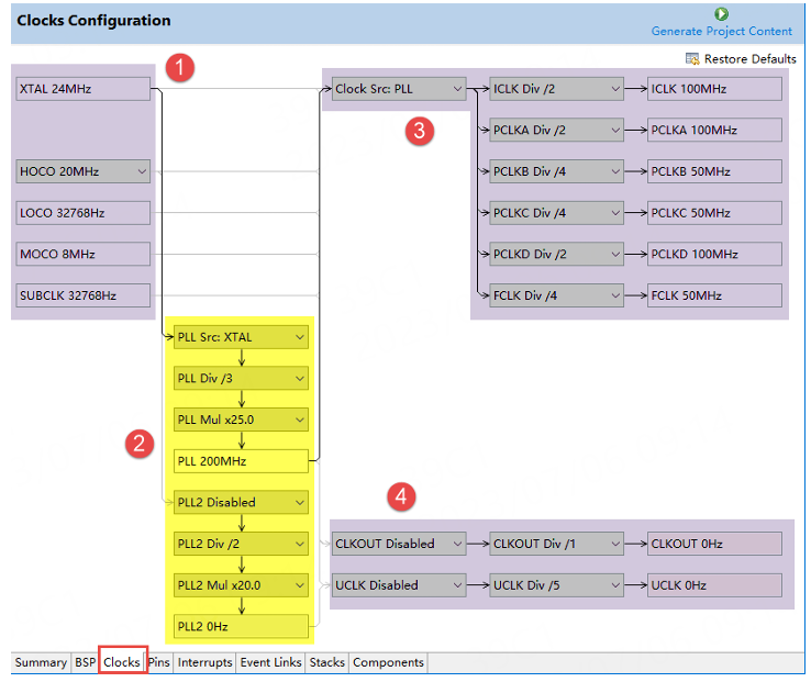
The default clock configuration for the RA4M2 in the FSP configurator is shown in the image below:
Click to view the full image
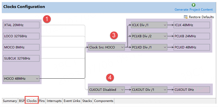
The above image is similar to the RA6M5 default clock configuration diagram and will not be elaborated further. The default clock configuration for the RA2L1 in the FSP configurator is shown in the image below:
Click to view the full image
In the above image, following the direction of the solid black arrows, it starts from “HOCO48Mhz”, which is the default choice of the internal high-speed oscillator (HOCO) of the chip. Of course, we can also change the configuration to select XTAL as the clock source, but we need to pay special attention to the fact that the external high-speed crystal oscillator connected to the Qiming 2L1 development board has a frequency of 8MHz, not the 20MHz default setting shown in the image. When selecting XTAL as the clock source, if the frequency of the external high-speed crystal oscillator is set incorrectly, the chip will not function, so this setting needs to be changed to “XTAL8MHz”. Continuing from HOCO, the system clock source selection (ClockSrc) is the on-chip high-speed oscillator (HOCO), which then provides clock lines and their attached peripherals through respective dividers. Note that the RA2L1 does not have a PLL.
Notes
For more detailed content on the clock tree, please refer to Figure 8.1 of Chapter 8 of the hardware manual, which illustrates the clock generation circuit diagram.
We can simply divide the above simplified clock tree (clock configuration diagram) into several areas, which are labeled with numbers in the diagram. Next, we will analyze the clock signals in these areas one by one.
-
①- Clock Source
-
②- Phase-Locked Loop
-
③- System Clock Area
-
④- Dedicated Independent Clock Area for Peripherals


Need Technical Support?
If you have any questions while using Renesas MCU/MPU products, you can scan the QR code below or copy the URL into your browser to access the Renesas Technical Forum for answers or to obtain online technical support.

https://community-ja.renesas.com/zh/forums-groups/mcu-mpu/
To be continued
Recommended Reading

Detailed Explanation of FSP Library Startup Files – Practical Guide to Renesas RA Series FSP Library Development (27)

SystemInit() – Practical Guide to Renesas RA Series FSP Library Development (28)
CGC Clock Control – Practical Guide to Renesas RA Series FSP Library Development (29)