Source: Content from ASML, thank you!
This article will take you through the chip manufacturing process.
Manufacturing a chip requires continuously layering patterns on a wafer, which can reach over 100 layers.
The chip manufacturing process involves hundreds of steps, and it may take four months from design to mass production. In the cleanroom of a wafer fab, precious wafers are continuously transported by mechanical equipment, and throughout the process, the air quality and temperature are strictly controlled.
How is a chip made?
Key processes in chip manufacturing (10 steps)
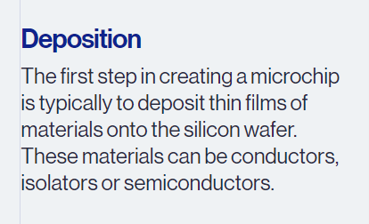
Deposition
The first step in chip manufacturing is typically to deposit a thin film of material onto the wafer. The materials can be conductors, insulators, or semiconductors.
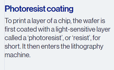
Photoresist Coating
Before photolithography, a photosensitive material called “photoresist” is coated onto the wafer, which is then placed in the photolithography machine.
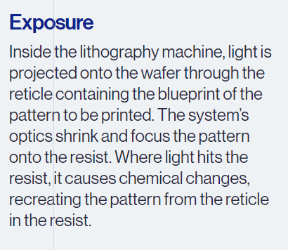
Exposure
A blueprint of the patterns to be printed is created on the mask. After the wafer is placed in the photolithography machine, a beam of light is projected through the mask onto the wafer. The optical components in the photolithography machine reduce and focus the pattern onto the photoresist layer. Under the beam’s exposure, a chemical reaction occurs in the photoresist, imprinting the pattern from the mask onto the photoresist layer.
Computational Lithography
The physical and chemical effects generated during lithography may cause pattern distortion, so adjustments are made to the patterns on the mask in advance to ensure the accuracy of the final lithographed pattern. ASML integrates existing lithography data and round wafer test data to create algorithm models for precise pattern adjustments.
Baking and Development
After the wafer leaves the photolithography machine, it undergoes baking and development to permanently fix the lithographed pattern. Excess photoresist is washed away, leaving some areas of the coating blank.
Etching
After development, gases and other materials are used to remove excess blank areas, forming a 3D circuit pattern.
Measurement and Inspection
During the chip production process, the wafer is continuously measured and inspected to ensure there are no errors. The inspection results are fed back to the lithography system for further optimization and adjustment of the equipment.
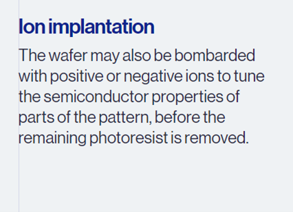
Ionic Implantation
Before removing the remaining photoresist, positive or negative ions can be used to bombard the wafer to adjust the semiconductor properties of certain patterns.
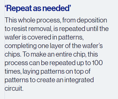
Repeat Process Steps as Needed
From film deposition to photoresist removal, the entire process covers the wafer with a layer of patterns. To form integrated circuits on the wafer and complete chip production, this process needs to be repeated many times, potentially up to 100 times.
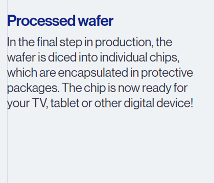
Chip Packaging
The final step involves cutting the wafer to obtain individual chips, which are then packaged in protective shells. This way, the finished chips can be used to produce televisions, tablets, or other digital devices!
Mini Skyscrapers
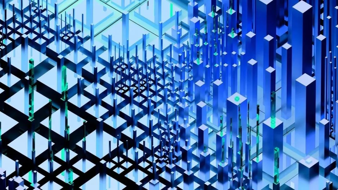
As mentioned above, the “repeat process steps as needed” means that modern chips can have structures with up to 100 layers, requiring nanometer-level precision for stacking, known as alignment accuracy. The sizes of the lithographed patterns on the chip vary, which means that different equipment is needed for the lithography of each layer. ASML’s DUV deep ultraviolet lithography machines come in several different models, suitable for critical lithography needs of the smallest patterns and normal lithography of standard patterns.
How Clean is Clean Enough?
It is important to know that no matter how small the dust or foreign objects are, once they land on the wafer, they can damage the chip. Moreover, some modern chips need to undergo dozens or even hundreds of layers of processes, so ensuring the yield of chip production is crucially dependent on the cleanliness of the wafer fab.
How clean is a cleanroom?
It is about 10,000 times cleaner than our everyday living spaces! Most chip manufacturers’ “ISO Class 1” cleanrooms can achieve almost “zero dust,” specifically, in every cubic meter of air, there are no more than 10 particles sized 100 to 200 nanometers, and no particles larger than 200 nanometers. In contrast, a clean modern hospital has about 10,000 dust particles per cubic meter of air, which is a significant difference.
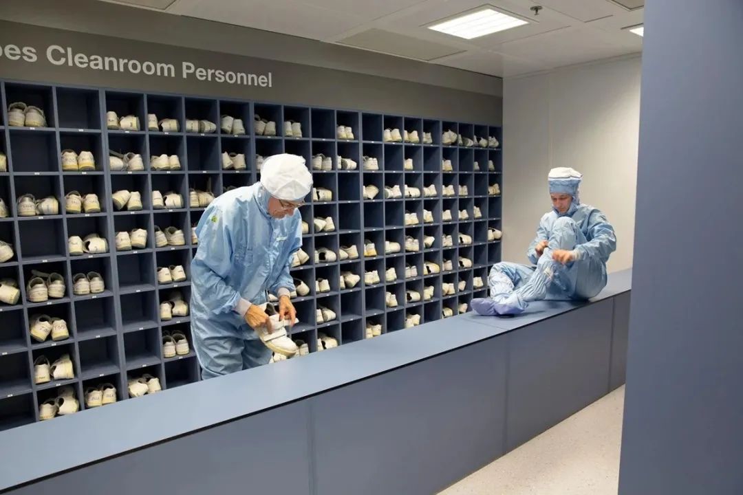
The air in the cleanroom is continuously filtered and circulated. Employees need to wear special work clothes (also known as “bunny suits”) to maintain a dust-free working environment.
ASML’s lithography machine factory is located in Veldhoven, Netherlands, and ASML’s equipment is also produced in cleanrooms.
Various Chip Manufacturing Models
IDMs design and manufacture chips simultaneously, with representative companies including Intel and Samsung. Foundries manufacture chips for other companies based on contracts, with representative companies including TSMC, GlobalFoundries, and UMC. Fabless companies do not own fabs, such as Qualcomm, NVIDIA, and AMD. They focus on chip design without involving production facility construction and maintenance, thus avoiding high costs. These companies may outsource production to foundries.
How are chips made? Finally, let’s listen to Scott Middlebrooks’ explanation.




E课网 (www.eecourse.com) is a professional integrated circuit education platform under Moores Elite, dedicated to training high-quality professional talent in the semiconductor industry. The platform is oriented towards the job demands of integrated circuit companies, providing practical training platforms that align with the corporate environment. Through online and offline training methods, it quickly cultivates students to meet corporate needs.
E课网 has a mature training platform, a comprehensive curriculum system, and strong teaching resources, planning 168 high-quality semiconductor courses in China, covering the entire integrated circuit industry chain, and has 4 offline training bases. So far, it has deeply trained a total of 15,367 people, directly supplying 4,476 professional talents to the industry. It has established deep cooperative relationships with 143 universities and has held 240 corporate-specific IC training sessions.