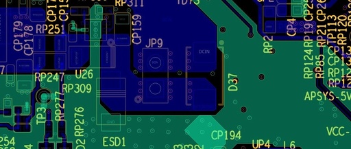
Surface Flatness Requirements for Gold Bonding Areas on Microwave Circuit Boards

Surface Flatness Requirements for Gold Bonding Areas on Microwave Circuit Boards

PCB Thermal Design: A Comprehensive Analysis from Theory to Practice Thermal issues are often the “Achilles’ heel” of many electronic products, especially in modern PCB designs with high integration and high power consumption. I remember a project I took on last year for an industrial control board, where the main chip had a power consumption … Read more

Understanding PCB Copper Pour: Benefits, Drawbacks, and Design Considerations

Understanding PCB Copper Pour: Benefits, Drawbacks, and Design Considerations

PCB Copper Pour refers to the area filled with copper in a PCB layer. This layer can be on the top, bottom, or any internal layer of the PCB, and PCB copper pour can be used for grounding, reference, or to isolate specific components or circuits from the rest of the elements on that layer. … Read more