

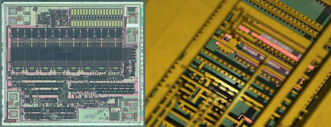
The “multi-layer” approach to chip manufacturing
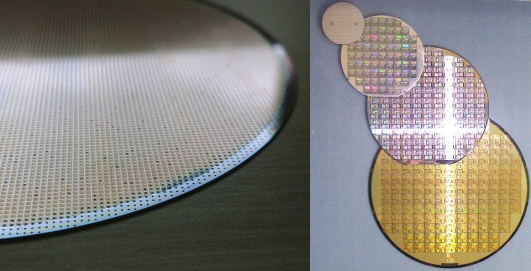


What limits the internal size of chips?

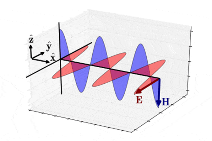
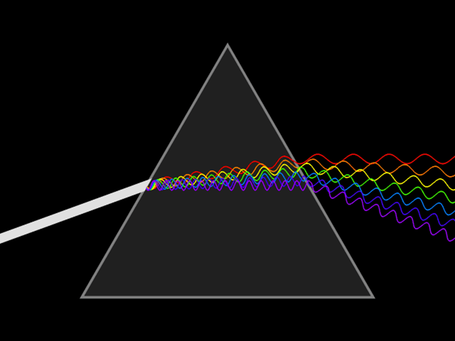
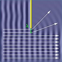
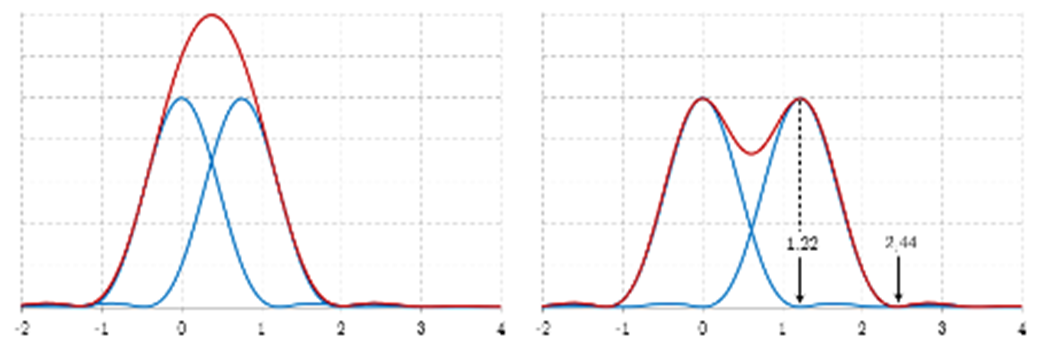
Diffraction
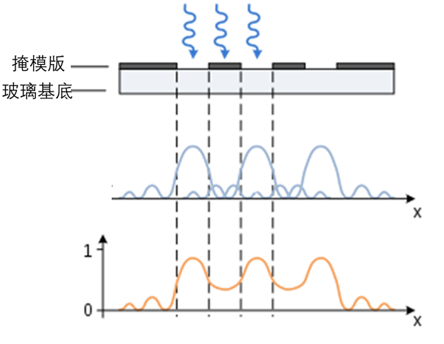
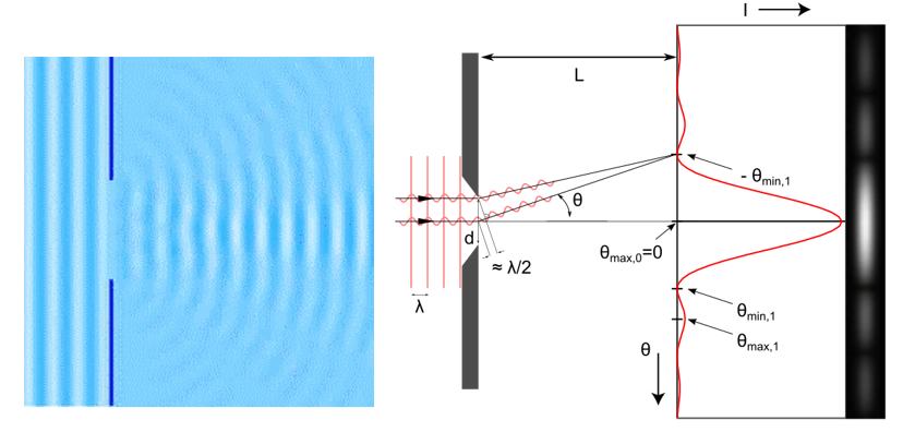

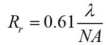
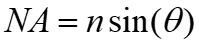
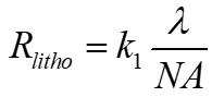
Resolution
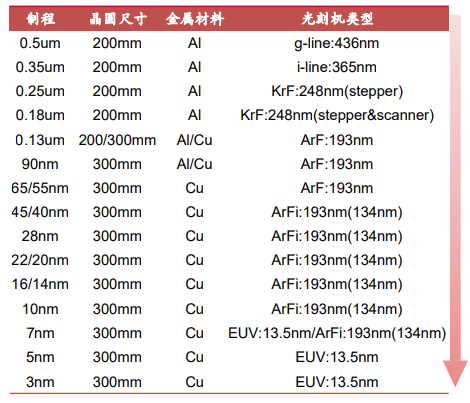
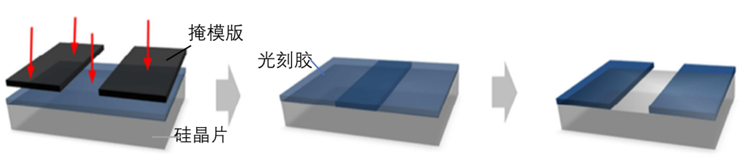
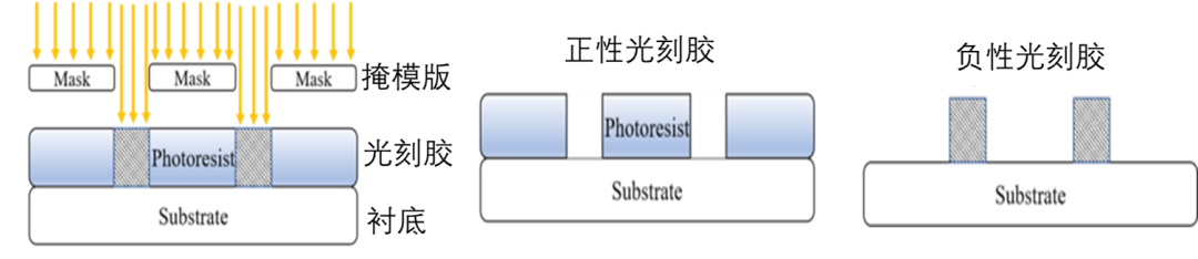
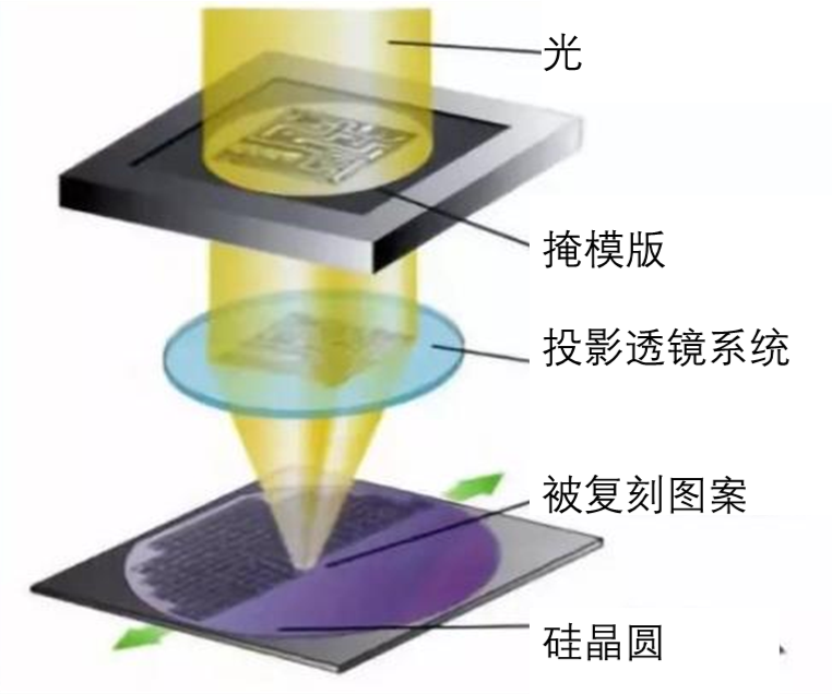
Photolithography
How to sharpen the light as a carving knife?
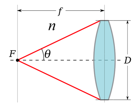
Increase the numerical aperture of the photolithography system
Shorten the wavelength
Reduce the process factor