When it comes to chips, many people’s first reaction might only be the CPU in a computer. So what exactly is a chip? Searching online, a chip refers to an integrated circuit, which is a way to miniaturize circuits (mainly including semiconductor devices, as well as passive components, etc.) in electronics, often manufactured on the surface of semiconductor wafers. In simple terms, a chip is a product formed by one or more integrated circuits on a semiconductor, and integrated circuits are not like the wire circuits we learned in high school, but rather some micro-circuits.
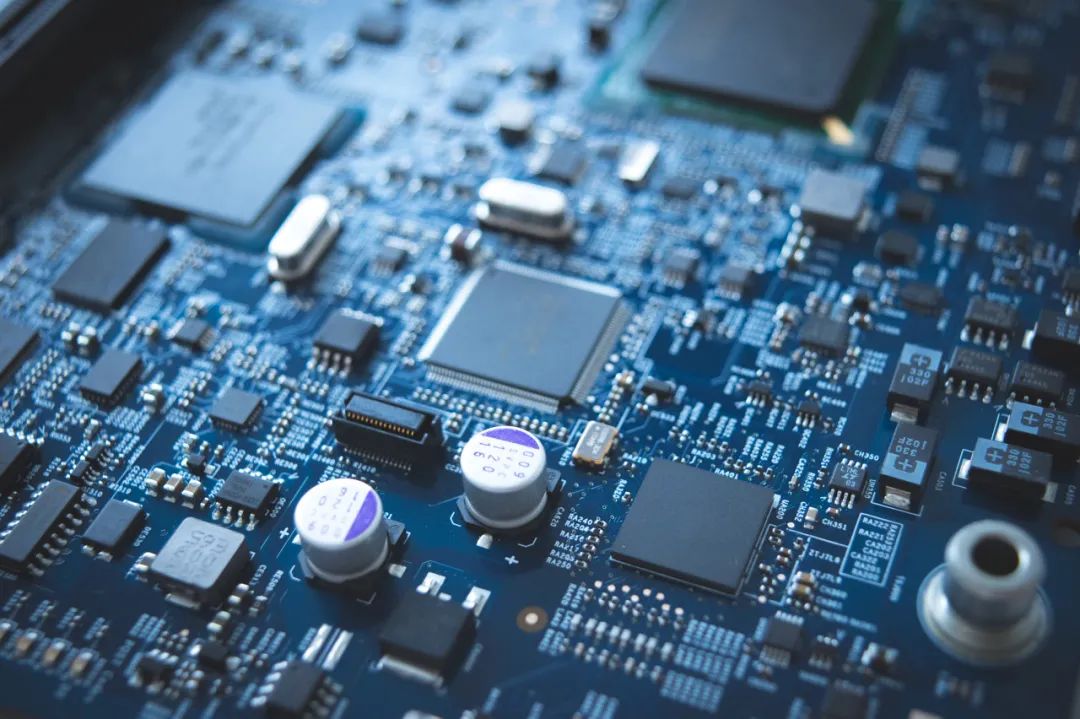
The motherboard composed of integrated circuits and chips. Image copyright, no unauthorized reproduction
The “core” of the chip refers to its importance. In modern society, many chips play the role of the “brain”; as the core of devices, the use of chips makes devices “smart.” The “chip” also represents its form, most chips are chip-shaped, which facilitates their integration into various devices.
The application of chips is very wide, so their classification is also quite complex. When mentioning chips, most people may simply equate chips with computer CPUs. However, the scope of what chips cover is much broader; the computer CPU is just one of the many functions that chips perform.
According to functionality, chips can be classified into four types:
-
Computing chips represented by the core CPU (Central Processing Unit) and GPU (Graphics Processing Unit);
-
Storage chips represented by memory chips such as ROM (Read-Only Memory) and DRAM (Dynamic Random Access Memory);
-
Sensing chips represented by camera core CMOS (Complementary Metal-Oxide-Semiconductor) chips;
-
Energy chips represented by AC/DC power management chips and communication chips represented by 5G, etc.
It can be said that all aspects of people’s daily lives are inseparable from chips.
Image copyright, no unauthorized reproduction
According to different application scenarios, chips can also be classified into consumer-grade, industrial-grade, automotive-grade, and military-grade chips. Apart from performance, their main differences lie in working temperature and environmental tolerance.
For example, the CPU of China’s Chang’e 4 has a computational speed that is only a fraction of your phone’s chip speed. You might wonder why such advanced lunar landing technology uses such a “slow” CPU? This is because the working environments of the two are different.
The phone chip comfortably “lies” on the motherboard, with stable room temperature, far from water and magnets, and equipped with heat sinks to prevent it from “overheating”; this working environment can be described as “comfortable.” We pamper it well, and it occasionally hangs up. In contrast, the CPU of Chang’e 4 operates in a space environment with temperature differences reaching 300°C, and it is constantly exposed to lethal cosmic radiation. Thus, the CPU of Chang’e 4 needs to be specially designed in terms of materials, systems, and structures, enabling it to “combat” the cosmic environment.
Therefore, for military products or aerospace equipment, ensuring the stability and reliability of chips under various complex environmental conditions is the most important consideration.
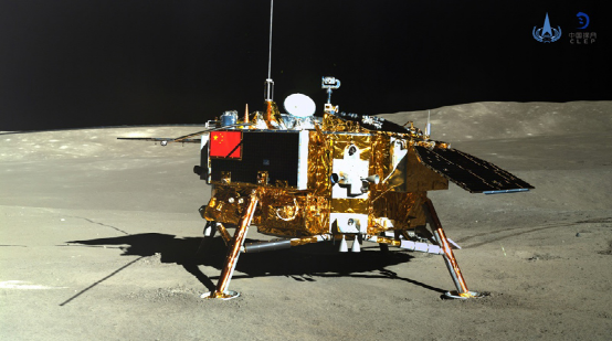
Chang’e 4, image source: Official website of the People’s Republic of China
Nowadays, the manufacturing process of chips is gaining more and more attention. The so-called “few-nanometer process” usually refers to the gate length of transistors in chips; the smaller the number, the higher the transistor integration density per unit area, and the stronger the performance. However, as the number of transistors in chips increases, the progress of human technology on CPUs has gradually slowed down, and the current processes and gate lengths can no longer match.
From Analog Signals to Digital Signals
Opening the Chapter of Digitalization in Nature
Things in nature are continuous, such as continuous time, continuous water flow, and “continuous” length. The initial inventions by scientists were also “continuous,” for example, wired telephones and wireless broadcasts directly transmit the same sound waves as the source, and early film photography relies on chemical materials for light sensitivity, similar to the frequency spectrum mapping of the human eye, thus producing images. This kind of “continuous” signal is called analog signal. Analog signals completely capture or restore nature, which seems to be a perfect technology. However, is reality really so?
During the transmission of signals, they undergo many processing and transfer stages, and in these processes, analog signals are susceptible to interference; at the same time, if the transmission is wired, electrical devices near the line can also produce electromagnetic interference. If it is wireless transmission, the open environment, due to more uncontrollable factors, makes analog signals nearly unusable, severely affecting communication quality. To this end, people have tried many methods to restore analog signals, but none can fundamentally solve the interference problem.

Image copyright, no unauthorized reproduction
However, later humans discovered that if continuous analog signals were converted into discrete digital signals, the problem would be easily solved. Although discrete digital signals inherently have errors and resolution compared to analog signals, digital signals have natural advantages in transportation, which can greatly alleviate signal interference and noise. Therefore, the problems that have troubled people for years have been solved.
From the moment digital signals were invented, the digitalization process of nature began. Want to obtain continuous images? Sure! Break the image into pixel blocks, then divide each pixel’s color into combinations of different brightness of red, green, and blue, and the image can be transformed into countless binary numbers. Want to obtain continuous sound? That’s possible too! First, discretize the continuous signal, then represent each part in binary, where the number of binary digits reflects the accuracy of the sound waveform, and finally encode it to become digital.
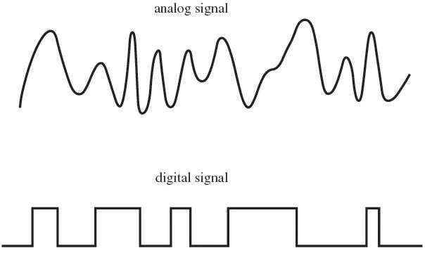
Analog signal (top) and digital signal (bottom)
Almost all objects in nature can be simulated in our digital world, ultimately leading the world to “1” and “0.” Thus, the saying “The world is yours, ours, but ultimately belongs to programmers” makes a lot of sense.
Semiconductors
The “Blank Paper” Where Chips Showcase Their Talents
Just as a poet’s rich literary talent needs to be expressed on a blank paper, the logical circuits on a chip also require such a “blank paper” to showcase their “strength.” Semiconductors—mainly silicon wafers made of high-purity silicon—serve as the “blank paper,” allowing circuit designers to freely express their wisdom and create various high-performance chips. Therefore, in chips, semiconductors and integrated circuits are equally important. But have you ever wondered why people choose semiconductors as the “blank paper”? Why did they choose silicon among many semiconductors?
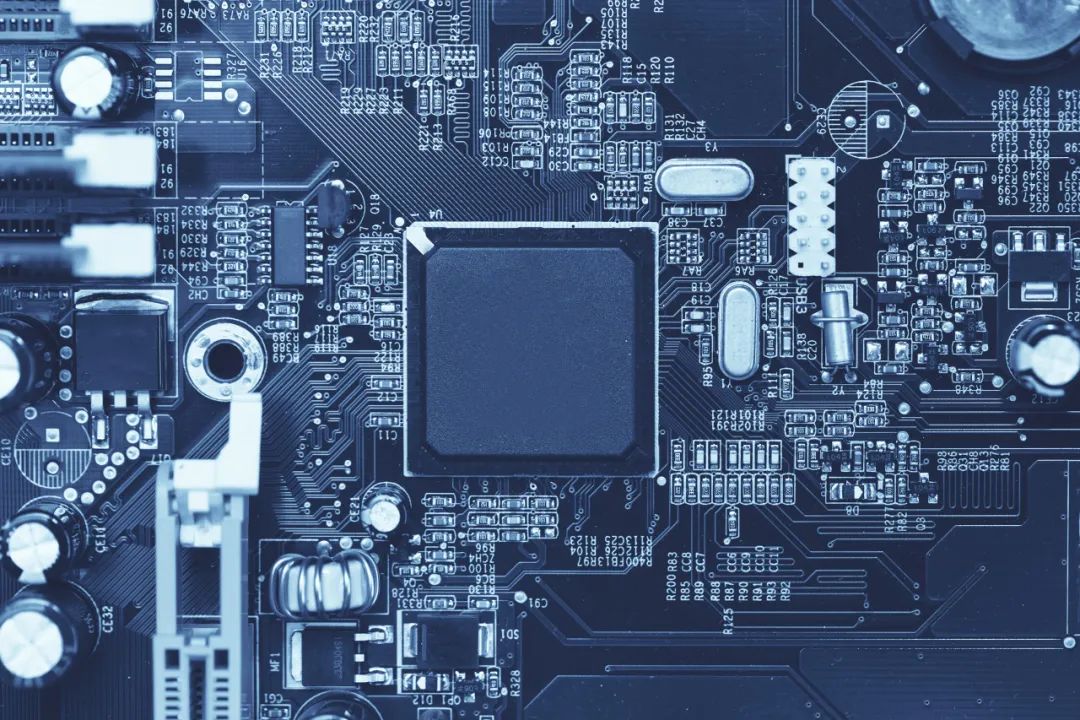
Image copyright, no unauthorized reproduction
Semiconductors have many magical properties, distinguishing them from conductors, which easily conduct electricity, and insulators, which hardly conduct electricity. Literally, semiconductors can be understood as materials with conductivity between conductors and insulators. However, semiconductors are far from simple; “half” is more about “change,” and their conductivity can change dramatically under varying conditions.
First is doping. Pure semiconductors are close to insulators, almost non-conductive. However, if doped, their conductivity increases sharply; if overdoped, they can even conduct electricity as easily as conductors. Additionally, doping with different atoms can give semiconductors either positive or negative charge, referred to as P-type semiconductors and N-type semiconductors. Based on these two types of semiconductors, scientists have created devices like diodes and transistors, which can be used to create arithmetic units capable of addition, subtraction, multiplication, and division, implement logic circuits like AND, OR, and NOT, and perform complex calculations.
Next is voltage. When P-type and N-type semiconductors come into contact, electrons inside them will form a “depletion layer” between the two types of semiconductors under the influence of electric fields or diffusion. When different directions of voltage are applied, the depletion layer thickens or thins, allowing the circuit to be turned on or off. This voltage-controlled on-off transformation is rapid, reversible, and can be repeated.
If we consider the circuit’s on state as “1” and the off state as “0,” we find that the on-off states of chips are surprisingly harmonious with digital signals. If the natural world can be composed of 0 and 1, then semiconductors are the brushes that build the world. Based on the magical properties of semiconductors, chips made from them can achieve all the functions you can imagine. Whether simulating an indistinguishable real world in games or creating artificial intelligence that closely resembles human thinking, chips can ultimately usher humanity into the digital age.

Image copyright, no unauthorized reproduction
The Best of Semiconductors—Silicon
Silicon is not a natural-born favorite. Initially, humans chose germanium as the chip material, and the entire industry has since been trying to find other semiconductors to replace silicon; gallium arsenide, gallium nitride, and other semiconductors emerged, but none could replace silicon’s dominant position in the chip industry. This is due to several significant advantages of silicon:
1. First, silicon is extremely abundant in nature. Silicon accounts for 28.6% of the Earth’s crust, widely found in rocks, gravel, and dust, second only to oxygen, and even ranks eighth in abundance in the universe.
2. Good doping properties. One of the advantages of semiconductors is their doping capability, and silicon is one of the most suitable materials for doping.
3. Additionally, silicon’s physical and chemical properties are relatively stable, making the chips less prone to damage.
4. Silicon also has excellent electron mobility. Mobility refers to the average drift velocity of charge carriers (electrons and holes) under the influence of an electric field, which is one of the decisive factors for the conductivity of materials. The higher the mobility, the lower the resistivity; with the same current, the power consumption is lower, and less heat is generated, thus increasing the current carrying capacity. In addition to low power consumption, high mobility also affects the operating frequency of devices. For example, the cutoff frequency of transistors is proportional to the carrier mobility, so increasing carrier mobility can improve the switching speed of transistors, thereby enhancing the performance of chips.
5. Furthermore, silicon has dense oxides—silicon dioxide. Silicon dioxide is insoluble in water and most acids, which perfectly aligns with printed circuit board technology, resulting in the current planar technology of integrated circuits.
6. Finally, silicon is easy to purify. After decades of research, we can now produce silicon with a purity of up to 99.999999999%, which is almost the purest material found in nature. Purification is crucial for chip manufacturing; as the number of transistors in a chip increases and the structure length reaches the nanoscale, the “blank paper” needed to create such precise structures must be as flat and white as possible. This means silicon wafers need to have high purity, high flatness, high cleanliness, and low impurity contamination properties to perfectly maintain the functionality of chip designs.
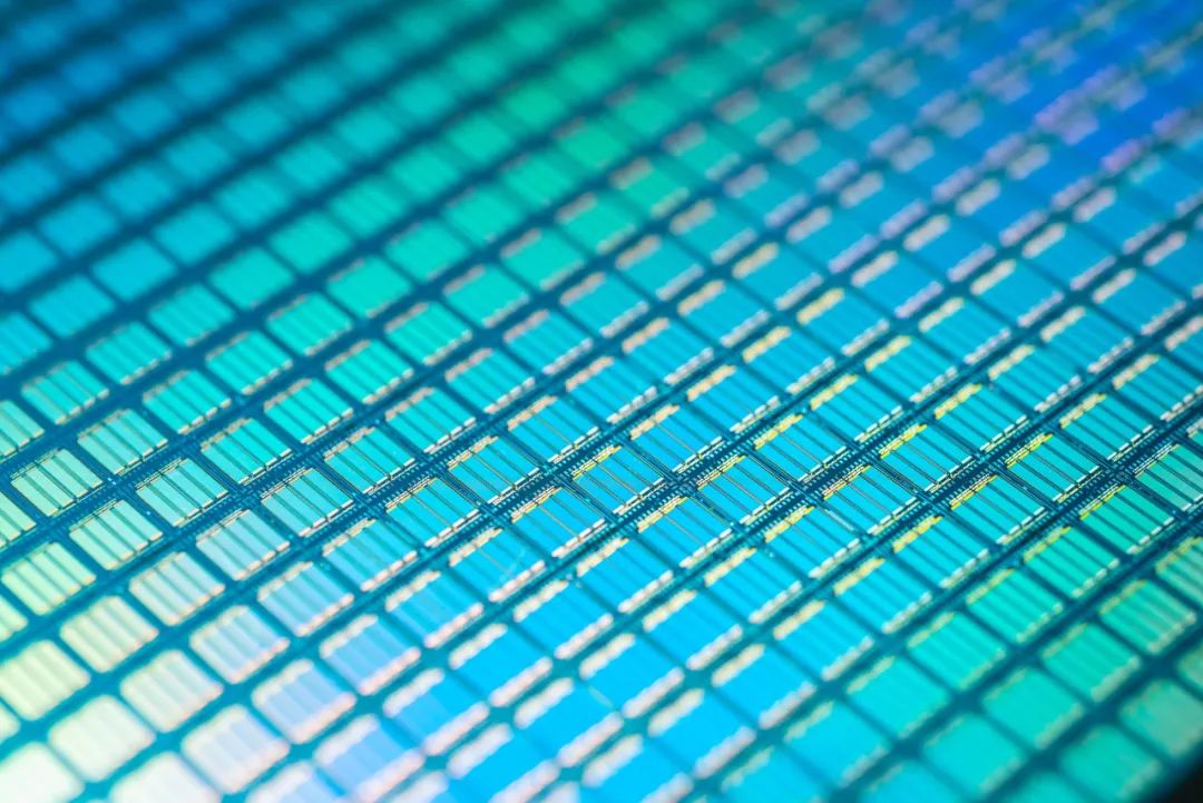
Silicon wafer, image copyright, no unauthorized reproduction
Having seen this, some may wonder, since the role of silicon wafers is so important, the manufacturing process must be quite difficult. In fact, the process of making silicon wafers is not hard, but how to produce such pure silicon wafers? Stay tuned for the next installment.
Produced by|Science Popularization China
Author|Wang Zhihao (Changchun Institute of Optics, Fine Mechanics and Physics, Chinese Academy of Sciences)
Supervised by|China Science Popularization Expo
Sent by|Computer Information Network Center, Chinese Academy of Sciences