Recently, due to a series of events, public interest in the domestic chip industry has been increasing.
So, what is a chip? How is it manufactured? What high technologies are involved? What is the current state of China’s chip industry? What challenges does it face?
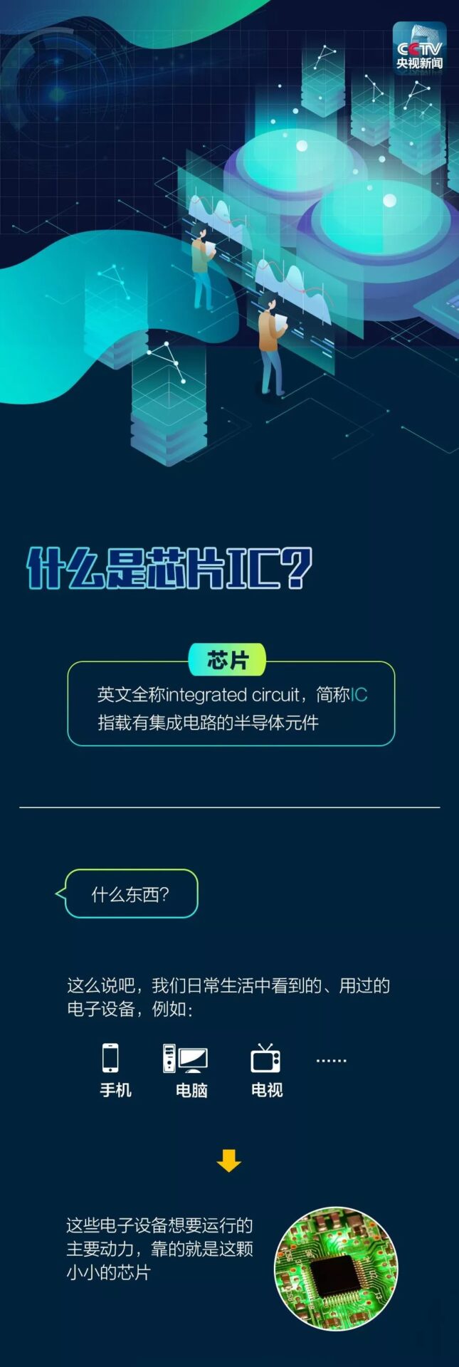
The essence of a chip is a semiconductor combined with integrated circuits, which is a miniaturization of circuits manufactured on a semiconductor wafer, a type of micro-circuit with special functions. Why is it called a chip? The term ‘chip’ refers to its shape, while ‘core’ signifies the heart, brain, or center of an electronic device, hence it is called a chip. This name has led many to misunderstand chips, thinking that only components like CPUs in computers are chips. The CPU in a computer is a logic chip that can control logic and has computational capabilities. However, there are many other types of chips, such as communication chips like 5G, Wi-Fi, and Bluetooth, as well as storage chips like those found in memory and USB drives, and sensor chips like gyroscopes in smartphones, etc.
Why must chips be semiconductors? Before semiconductors, humans could only control electricity mechanically, but with semiconductors, we can directly control electricity with electricity, achieving a qualitative leap in control capabilities. The development of quantum mechanics in the early 20th century led to the discovery of semiconductors as a key material. By merely applying voltage changes, we can switch between semiconductor and insulator states, which transitioned humanity from the electrical age to the electronic age.
With semiconductors, humans can finally use this advanced physical form of electricity to control this advanced energy form, greatly enhancing our ability to process information. Thus, chips must be made of semiconductor materials, which is fundamentally why chips opened the information age.
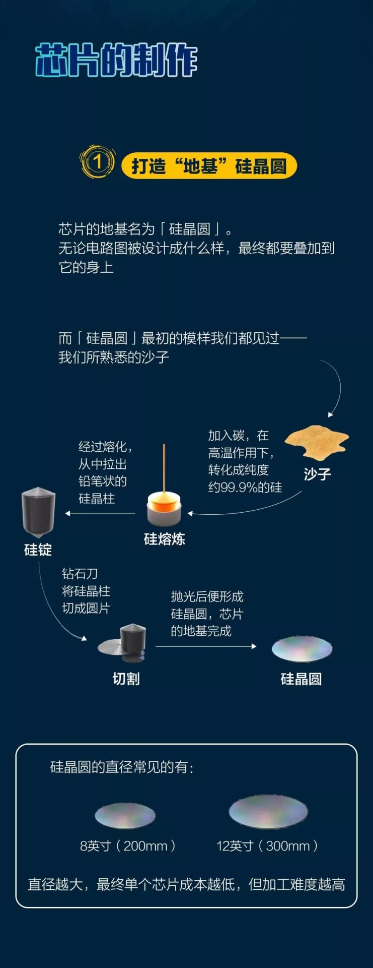
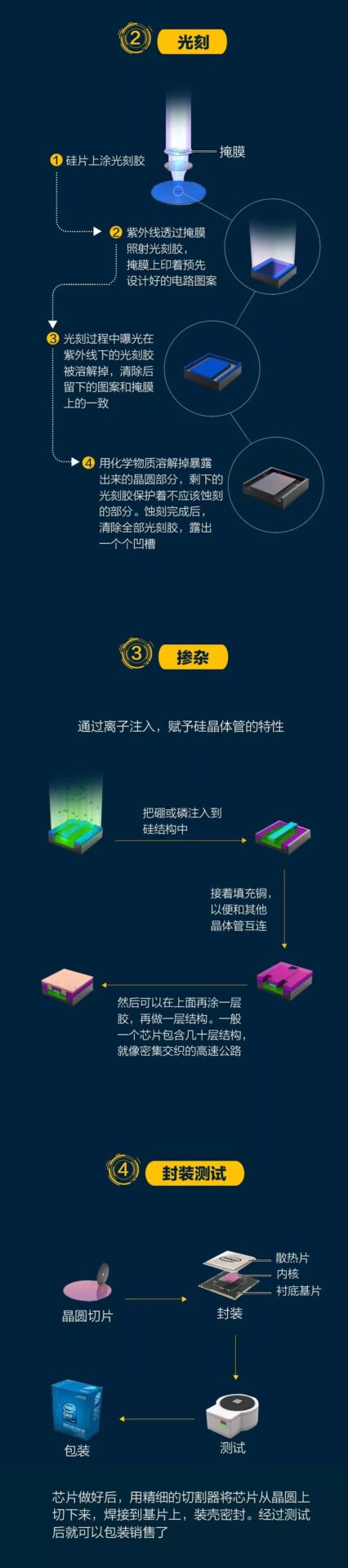
Another essential aspect of chips is integrated circuits. In the past, humans assembled individual components by soldering them together; now, technology resembles micro-sculpting, directly carving these circuits onto a very small object. This very small object is the semiconductor substrate, and the carving tool is the photolithography machine, which uses lasers instead of metal blades, and is extremely fine.
Currently, it is possible to carve at the nanometer scale, integrating over 10 billion transistors onto a chip the size of a square centimeter, which is far more complex than you can imagine.
Here, we will share a popular science article from CCTV News:
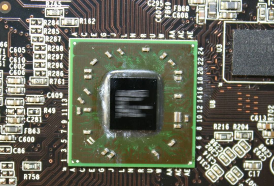
Despite the small size of chips, the manufacturing difficulty is enormous, and the process is no less than building a city on a fingernail. The chips we usually see look like this:
However, under a microscope, it resembles a sprawling network of streets, with countless details that are astonishing.
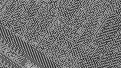
It turns out that a chip the size of a fingernail has several kilometers of wiring and tens of millions or even billions of transistors.
To allow these nanoscale components to “settle down,” chips must undergo hundreds of nanometer-level transformations before they can be put into use…
1. The Complex and Tedious Chip Design Process
The process of chip manufacturing is akin to building a house with Lego blocks; first, you have the wafer as the foundation, then the chip manufacturing process is layered on top, resulting in the necessary IC chips. However, without a design blueprint, even the strongest manufacturing capabilities are useless, so we will now introduce IC design.
In the IC production process, ICs are usually planned and designed by specialized IC design companies. Well-known companies like Huawei HiSilicon, MediaTek, Qualcomm, and AMD design their own IC chips, providing different specifications and performance options for downstream manufacturers. Since ICs are designed by various companies, IC design heavily relies on the skills of engineers, and the quality of engineers affects the value of a company. However, what steps do IC design engineers take when designing an IC chip?
Step One: Define Objectives
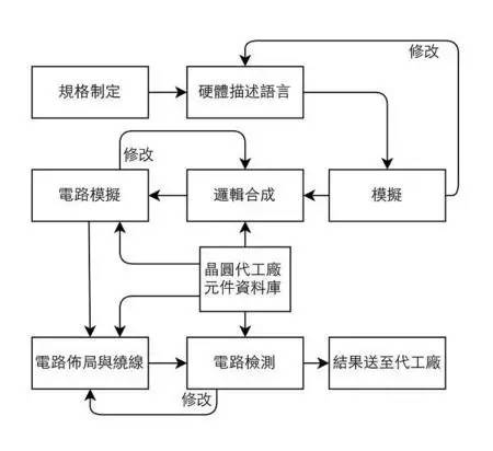
In IC design, the most important step is specification formulation. This step is like deciding how many rooms and bathrooms are needed before designing a building, and what building regulations must be followed. After confirming all functions, design can proceed, avoiding extra time for subsequent modifications. IC design also requires similar steps to ensure that the designed chip will have no errors.
The first step in specification formulation is to determine the purpose and performance of the IC, setting the overall direction. Next, check what protocols need to be complied with. For example, a wireless network card chip must comply with IEEE 802.11 standards; otherwise, the chip produced will not be compatible with market products, making it unable to connect with other devices. Finally, establish the production methods for the IC, distributing different functions into various units and defining how these units will connect, thus completing the specification formulation.
Once the specifications are set, the next step is to design the details of the chip. This step is like making initial notes on the building’s plan, sketching the overall outline for future drafting. In IC chips, this involves using Hardware Description Language (HDL) to describe the circuits. Commonly used HDLs include Verilog and VHDL, which allow easy expression of an IC’s functions. The next step is to check the correctness of these codes and continuously modify them until they meet the expected functionality.

▲ Example of a 32-bit adder in Verilog
With Computers, Things Become Easier
With a complete plan in place, the next step is to create a flat design blueprint. In IC design, the logic synthesis step involves inputting the verified HDL code into EDA tools, allowing the computer to convert the HDL code into logic circuits, producing the following circuit diagram. Afterward, the design must be repeatedly verified to ensure it meets specifications and modified until the functionality is correct.
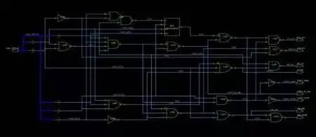
▲ Result after synthesizing the control unit
Finally, the synthesized code is placed in another set of EDA tools for circuit layout and routing (Place And Route). After continuous testing, the following circuit diagram is formed. The diagram shows different colors like blue, red, green, and yellow; each color represents a different photomask. During chip production, this diagram is used to layer the chip starting from the bottom.
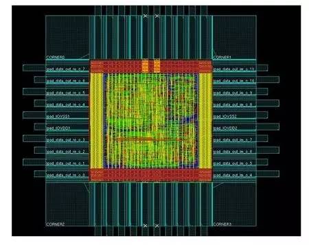
▲ Commonly used computational chip – FFT chip, completed circuit layout and routing results
At this point, everyone should have a preliminary understanding of IC design. Overall, it is clear that IC design is a very complex specialty, and thanks to the maturity of computer-aided software, IC design has been accelerated.
2. How Are Chips Manufactured?
The wafer is the foundation for manufacturing various chips. We can liken chip manufacturing to building a house with Lego blocks, stacking layer upon layer to achieve the desired shape (various types of chips).
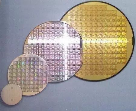
▲ Comparison of wafers of various sizes
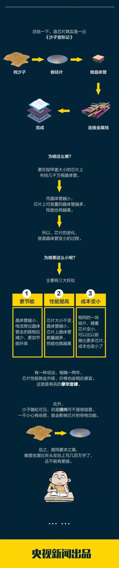
Chips, made from the most abundant and cost-effective silicon dioxide, have achieved the pinnacle of technology on this planet, deserving of the best comeback award!
So, what stage is China’s “chip” currently at? What problems does it face?