In today’s electronic devices, there is an increasing demand for high performance, low power consumption, and miniaturization, which places higher requirements on the design of power management chips. The LPK8727, as a 12W simplified self-powered primary-side feedback control chip, has become an ideal choice for many power design engineers due to its high integration, simple peripheral design, and excellent performance. This article will delve into the technical specifications, typical applications, and design points of the LPK8727 chip, providing detailed references for engineers in related fields.
Overview of the LPK8727 Chip
The LPK8727 is a highly integrated self-powered primary-side feedback control chip for isolated adapters and chargers. This chip is designed for isolated solutions under 12W, with extremely simple peripheral circuits, greatly simplifying system design and reducing costs. The LPK8727 allows for adjustable primary peak current through an external resistor and sets the output constant current point via the turns ratio of the transformer. Additionally, the output constant voltage point can be precisely set by configuring the bias resistor on the feedback pin (FB).
Technical Specifications
(1) Basic Features
Integrated BJT: Suitable for isolated solutions under 12W. Built-in startup circuit: No external startup resistor is required, simplifying the startup process. Self-powered technology: Eliminates the auxiliary winding VCC power diode, further reducing system costs. Adjustable peak current: Peak current can be adjusted through an external resistor, providing flexible design options. Ultra-low standby power consumption: Effectively reduces energy consumption in standby mode. Patented current drive technology: Reduces temperature rise and improves system stability. Output line loss compensation technology: Adjusts the output cable compensation value by setting the value of the external upper bias resistor on FB, improving output voltage accuracy. Comprehensive protection features: Includes VCC clamping/under-voltage protection, FB pin resistor open-circuit protection, output short-circuit protection, output over-voltage protection, and over-temperature protection.
(2) Electrical Parameters
Power supply voltage (VCC): -0.3V to 6.5V. Feedback voltage input (FB): -0.3V to 6.5V. Peak current selection pin (SEL): -0.3V to 6.5V. Maximum power consumption (DMAX): 0.45W. Thermal resistance from junction to ambient (θJA): 120℃/W. Thermal resistance from junction to case (θJC): 40℃/W. Operating junction temperature range (TJ): -40℃ to 150℃. Storage temperature range (TSTG): -55℃ to 150℃. ESD protection: 2KV (human model).
(3) Package Information
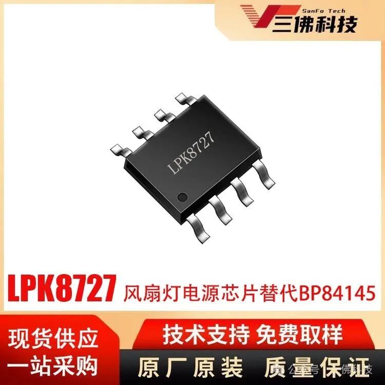
The LPK8727 is packaged in SOP8L, featuring good heat dissipation and compact size, suitable for various compact power designs.
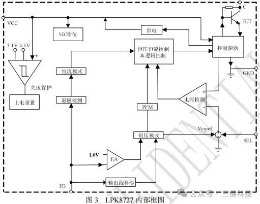
(4) Internal Block Diagram
Typical Applications
(1) Adapters and Chargers
The LPK8727 is particularly suitable for various adapter and charger applications, providing stable output voltage and current, ensuring the safety and reliability of devices during the charging process. Its built-in multiple protection features, such as output short-circuit protection and over-voltage protection, effectively prevent damage to devices due to abnormal conditions.
(2) LED Driver Power Supplies
In LED driver power supplies, the LPK8727 can provide precise constant current control, ensuring that LEDs maintain stable brightness under different operating conditions. Its output line loss compensation technology effectively compensates for the voltage drop due to output line losses, improving the overall efficiency of the system.
(3) Upgrading Linear Power Supplies and RCC Switching Power Supplies
The LPK8727 can serve as an upgrade for linear power supplies and RCC switching power supplies, offering higher efficiency and better performance. Its self-powered technology and built-in startup circuit simplify design and reduce system costs.
(4) Other Auxiliary Power Supplies
The LPK8727 is also suitable for various auxiliary power supply applications, such as backup power for small electronic devices. Its low standby power consumption and comprehensive protection features make it an ideal power management solution.
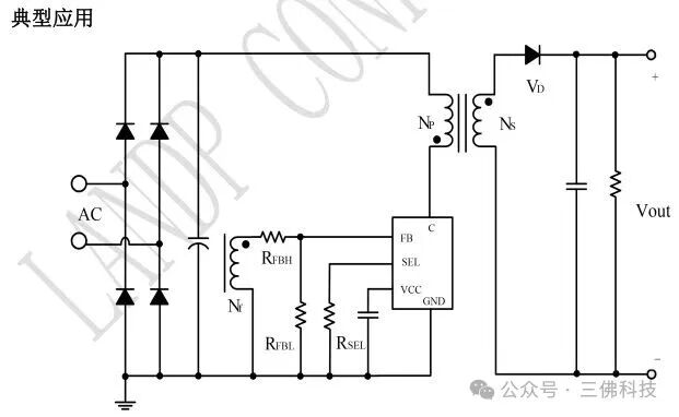
The typical application diagram of the LPK8727 is shown below:
Design Points
(1) Startup Process
The LPK8727 requires only 1uA of startup current. After the system is powered on, the internal startup circuit charges the capacitor at Vcc. When the Vcc voltage reaches the chip’s turn-on threshold, the internal control circuit of the chip begins to operate. After the system starts, Vcc is powered by the internal proprietary power supply circuit.
(2) Peak Current Setting
The SEL pin is connected to an external resistor RSEL, which can adjust the maximum peak current IPKMAX. The formula is as follows: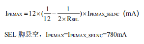
It is recommended that RSEL > 15K.
(3) Constant Current Control
The LPK8727 detects the peak current of the inductor on a per-cycle basis. When the real-time current in the primary-side inductor exceeds the maximum peak current IPKMAX set by the chip, the power transistor turns off. The output current IOUT calculation formula is as follows: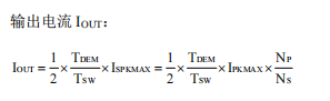
Where TDEM is the demagnetization time, TSW is the switching period, ISPKMAX is the secondary peak current, and IPKMAX is the primary peak current, NP is the number of turns in the primary of the transformer, and NS is the number of turns in the secondary of the transformer.
(4) Constant Voltage Control
The LPK8727 samples the feedback voltage through a resistor, and the voltage obtained after resistor division is compared with the internal reference to form a closed loop to maintain the output voltage Vout. The light load output voltage calculation formula is as follows:
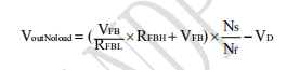
The loaded output voltage calculation formula is as follows:

Where RFBH is the upper bias resistor connected to FB, RFBL is the lower bias resistor connected to FB, ICOMP_LINE is the output line compensation current through the upper bias resistor at full load, Nf is the number of turns in the auxiliary winding, VFB is the reference voltage (typical value 1.0V), VD is the voltage drop across the output freewheeling diode, IO is the load current, and IOCP is the output constant current.
(5) Protection Features
The LPK8727 integrates various protection features, including: VCC clamping/under-voltage protection: Ensures the chip operates safely under abnormal voltage conditions. FB pin resistor open-circuit protection: Prevents system anomalies caused by external resistor failures. Output short-circuit protection: Protects the system from damage during output short circuits. Output over-voltage protection: Prevents excessive output voltage from damaging load devices. Over-temperature protection: Automatically shuts down when the chip temperature is too high to prevent thermal damage.
(6) PCB Design
When designing the PCB for the LPK8727, the following guidelines should be followed: VCC bypass capacitor: The bypass capacitor for VCC should be placed close to the chip’s VCC and GND pins. SEL pin resistor: The resistor for the SEL pin should be placed close to the chip’s SEL and GND pins. FB pin: The voltage divider resistors connected to the FB pin must be close to the FB pin, and the nodes should be far from the active points of the primary winding of the transformer. Power loop area: Minimize the area of the power loop, such as the loop area of the primary winding of the transformer, power transistor, and bus capacitor, as well as the loop area of the secondary winding of the transformer, rectifier diode, and output capacitor, to reduce EMI radiation. C pin: Appropriately increase the copper area of the C pin to improve chip heat dissipation.
Shenzhen Sanfo Technology provides samples and technical support!
Conclusion
The LPK8727, as a 12W simplified self-powered primary-side feedback control chip, has become an ideal choice for many power design engineers due to its high integration, simple peripheral design, and excellent performance.