Technology is advancing rapidly, with the Internet of Things, artificial intelligence, deep learning, and various chip terms like GPU, TPU, NPU, and DPU emerging one after another… What are they? And what are the differences?
01
CPU
The CPU, as the “brain” of the machine, is the “commander-in-chief” that strategizes, issues orders, and controls actions, bearing the core tasks of the entire computer system.
The CPU consists of multiple structures, including the Arithmetic and Logic Unit (ALU), Control Unit (CU), Register, and Cache, which communicate through data, control, and status buses. These structures and communication methods are essential for the CPU to complete various tasks and are key factors in improving computer processing efficiency.
In simple terms: The CPU architecture consists of three parts: computational units, control units, and storage units, as shown in the figure below: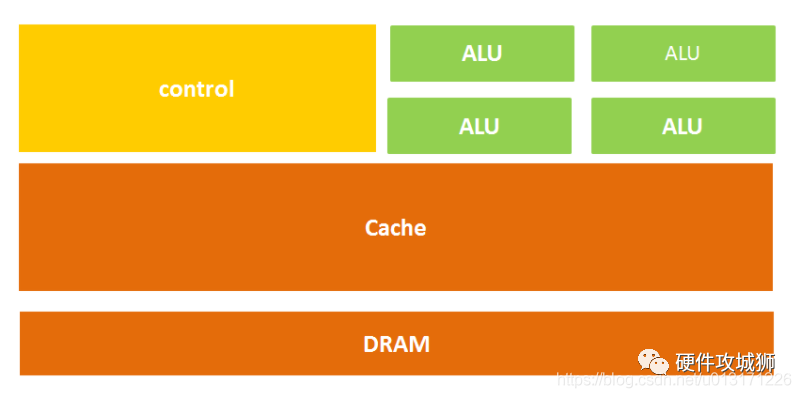
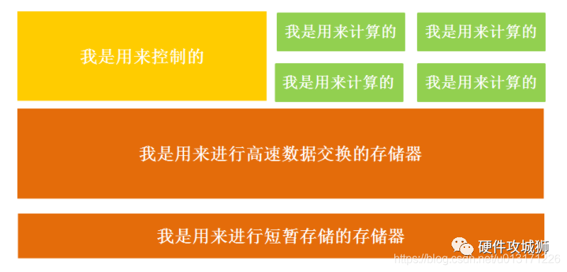
Literally, it’s easy to understand: the computational unit mainly performs arithmetic operations, shifts, and address calculations and conversions; the storage unit is mainly used to save data and instructions generated during computations; the control unit decodes instructions and issues control signals for executing various operations required to complete each instruction.
Thus, the process of executing an instruction in the CPU is as follows: after reading the instruction, it is sent to the controller (yellow area) for decoding via the instruction bus, which then issues the corresponding operational control signals; the ALU (green area) then calculates the data according to the operation instruction and stores the resulting data in the data cache (large orange area) via the data bus. The process is illustrated in the figure below:
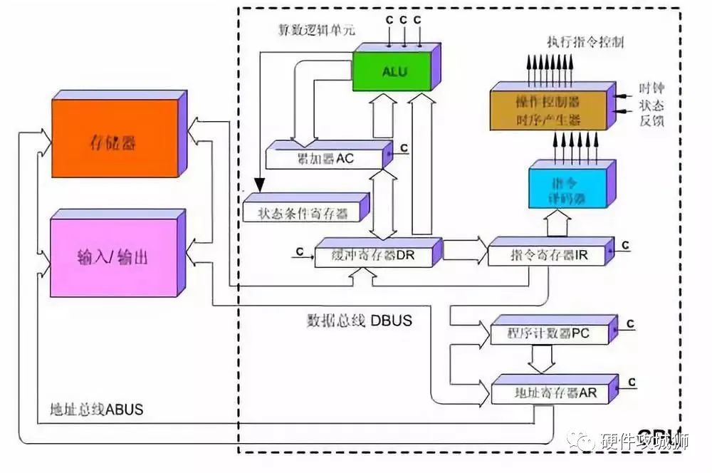
Figure: Diagram of CPU instruction execution
The CPU follows the Von Neumann architecture, which is fundamentally about: storing programs and executing them sequentially. In this structure diagram, the green area responsible for computation seems too small, while the orange area (Cache) and yellow area (Control Unit) occupy a large amount of space.
Because the CPU architecture requires a lot of space to accommodate storage units (orange part) and control units (yellow part), compared to which the computational unit (green part) occupies only a small portion, it is severely limited in large-scale parallel computing capabilities and is better suited for logical control.
Moreover, because it follows the Von Neumann architecture (storing programs and executing sequentially), the CPU behaves like a meticulous housekeeper, executing tasks step by step as instructed. However, as the demand for larger scale and faster processing speeds increases, this housekeeper gradually becomes overwhelmed.
Thus, can we place multiple processors on the same chip to work together, thereby improving efficiency? This led to the birth of the GPU.
02
GPU
GPU stands for Graphics Processing Unit, which is a microprocessor used for performing graphical calculations in personal computers, workstations, game consoles, and some mobile devices (such as tablets and smartphones). As the name suggests, the GPU was originally designed for graphical processing tasks.
Why is the GPU particularly good at processing image data? This is because every pixel point in an image needs to be processed, and the process and method for processing each pixel point are quite similar, making it a natural fit for the GPU.
The simple architecture of the GPU is shown in the figure below:
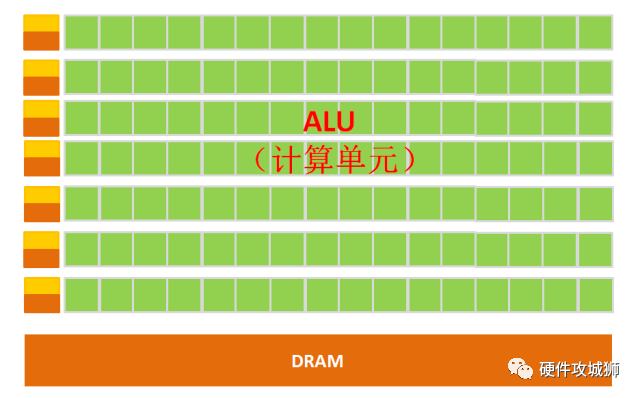
Figure: GPU microarchitecture diagram
From the architecture diagram, we can clearly see that the GPU’s structure is relatively simple, with a large number of computational units and very long pipelines, making it particularly suitable for processing large amounts of uniform-type data.
However, the GPU cannot work independently; it must be controlled and invoked by the CPU to operate. The CPU can work independently, handling complex logical operations and different data types, but when a large amount of uniform-type data processing is needed, the GPU can be called upon for parallel computation.
Note: The GPU has many ALUs and very few caches; the purpose of the cache is not to store data that will be accessed later, which is different from the CPU, but to improve service for threads. If many threads need to access the same data, the cache will merge these accesses and then access the DRAM.
Comparing the CPU and GPU side by side makes the differences very clear.
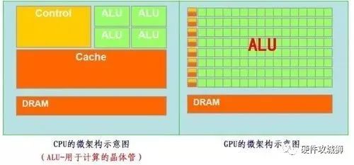
Most of the work done by the GPU involves a large amount of computation but lacks technical complexity, and it needs to be repeated many times.
To borrow a saying from a certain expert on Zhihu, it’s like having a job that requires calculating billions of additions and subtractions within a hundred. The best way is to hire dozens of elementary school students to do it together, each doing a part, as these calculations are not technically demanding—purely physical labor; whereas the CPU is like an old professor who can do integrals and derivatives but commands a high salary. One old professor is worth twenty elementary school students. If you were Foxconn, who would you hire?
The GPU uses many simple computational units to complete a large number of computational tasks, purely a strategy of manpower. This strategy is based on the premise that the work of elementary student A and elementary student B is independent of each other.
One point to emphasize is that although the GPU was born for image processing, we can see from the previous introduction that its structure does not have components specifically designed for image service; it merely optimizes and adjusts the CPU’s structure. Therefore, the GPU can not only excel in image processing but is also used in scientific computing, cryptography, numerical analysis, and massive data processing (sorting, Map-Reduce, etc.), and financial analysis, all requiring large-scale parallel computation.
Thus, the GPU can also be considered a relatively general-purpose chip.
03
TPU
As mentioned above, both the CPU and GPU are relatively general-purpose chips, but there is a saying: the efficiency of a universal tool will never match that of a specialized tool.
As people’s computational needs become more specialized, there is a desire for chips that better meet specific professional needs, leading to the concept of ASIC (Application-Specific Integrated Circuit).
ASIC refers to special specification integrated circuits customized according to different product needs, designed and manufactured based on the requirements of specific users and specific electronic systems. Of course, this concept doesn’t need to be memorized; simply put, it’s a customized chip.
Because ASICs are very “specialized” and only do one thing, they outperform general-purpose chips like CPUs and GPUs in specific tasks, achieving higher processing speeds and lower power consumption. However, correspondingly, the production cost of ASICs is also very high.
The TPU (Tensor Processing Unit) is a chip developed by Google specifically to accelerate the computational capabilities of deep neural networks, which is essentially an ASIC.
Initially, many machine learning and image processing algorithms ran on GPUs and FPGAs (field-programmable gate arrays), but these two types of chips are still general-purpose chips, so their performance and power consumption cannot be closely adapted to machine learning algorithms. Google has always believed that great software will shine even brighter with the help of great hardware, so they wondered if they could create a dedicated chip for machine learning algorithms, leading to the birth of the TPU.
It is said that the TPU can provide a performance increase of 15-30 times compared to CPUs and GPUs of the same period, and an efficiency increase (performance/watt) of 30-80 times. The first-generation TPU could only perform inference and relied on Google Cloud to collect data and generate results in real-time, while the training process required additional resources; the second-generation TPU can be used for both training neural networks and inference.
You might wonder why the TPU is so powerful in terms of performance?
Well, Google has written several papers and blog posts explaining this, so I’ll just touch on it here.
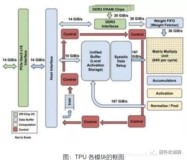
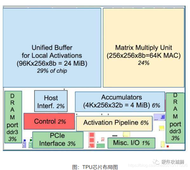
As shown in the figure above, the TPU uses up to 24MB of local memory, 6MB of accumulator memory, and memory for interfacing with the main processor, accounting for 37% of the chip area (the blue part in the diagram).
This indicates that Google fully recognizes that external memory access is the culprit behind the low energy efficiency of GPUs, so they spared no expense to include large memory on the chip. In contrast, NVIDIA’s K80 at the same time only had 8MB of on-chip memory, requiring constant access to external DRAM.
Additionally, the TPU’s high performance also comes from its tolerance for low computation precision. Research has shown that the accuracy loss from low-precision computation is minimal, but it can bring enormous convenience in hardware implementation, including lower power consumption, faster speeds, smaller computational units, and lower memory bandwidth requirements… The TPU uses 8-bit low-precision computation.
So far, the TPU has already accomplished many tasks, such as the machine learning AI system RankBrain, which helps Google process search results and provide more relevant search results for users; the Street View system, which improves the accuracy of maps and navigation; and of course, the computer program AlphaGo that plays Go!
04
NPU
At this point, I believe everyone has a certain understanding of these so-called “XPUs”. Let’s continue.
The so-called NPU (Neural Network Processing Unit) is a neural network processor. As the name suggests, this chip aims to simulate human neurons and synaptic structures using circuits!
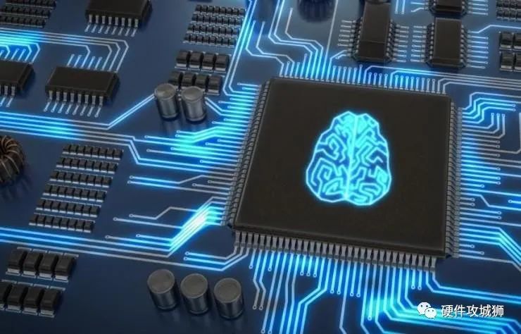
How to imitate? First, we need to take a look at the human neural structure—biological neural networks are composed of several interconnected artificial neuron nodes, with neurons connected to each other through synapses, which record the connections between neurons.
If we want to use circuits to simulate human neurons, we must abstract each neuron as an activation function, whose input is determined by the outputs of the connected neurons and the synapses connecting the neurons.
To express specific knowledge, users typically need to adjust the values of synapses and the topology of the network (through certain specific algorithms). This process is called “learning”.
After learning, the artificial neural network can solve specific problems using the acquired knowledge.
At this point, you may have noticed a problem—due to the basic operations of deep learning being the processing of neurons and synapses, while traditional processor instruction sets (including x86 and ARM) were developed for general computing, their basic operations are arithmetic operations (addition, subtraction, multiplication, division) and logical operations (AND, OR, NOT), often requiring hundreds or even thousands of instructions to complete the processing of a single neuron, leading to low efficiency in deep learning processing.
This necessitates a new approach—breaking through the classic Von Neumann structure!
In neural networks, storage and processing are integrated, both reflected through synaptic weights. In contrast, in the Von Neumann structure, storage and processing are separated, implemented by memory and arithmetic units respectively, leading to significant differences. When using existing classical computers based on the Von Neumann structure (like X86 processors and NVIDIA GPUs) to run neural network applications, they inevitably face constraints from the separation of storage and processing, which affects efficiency. This is one of the reasons why specialized chips designed for artificial intelligence have a certain inherent advantage over traditional chips.
05
ASIC
ASIC (Application Specific Integrated Circuit) is an integrated circuit designed for a specific purpose. It cannot be reprogrammed, has high performance and low power consumption, but is expensive. Recently, various dazzling chips such as TPU, NPU, VPU, and BPU have emerged, all of which essentially belong to ASIC. ASIC differs from the flexibility of GPUs and FPGAs; once a customized ASIC is manufactured, it cannot be changed, so the high initial costs and long development cycles create a high entry barrier. Currently, most participants are giants with AI algorithms and expertise in chip development, such as Google’s TPU. ASICs are perfectly suited for neural network-related algorithms, outperforming GPUs and FPGAs in terms of performance and power consumption; TPU1 is 14-16 times the performance of traditional GPUs, and NPU is 118 times that of GPUs. Cambricon has released an external application instruction set, and ASIC is expected to be the core of future AI chips.
06
BPU
(Brain Processing Unit)

Proposed by Horizon Robotics, it is an embedded artificial intelligence processor architecture. The first generation is the Gaussian architecture, the second generation is the Bernoulli architecture, and the third generation is the Bayesian architecture. Horizon has already designed the first generation of Gaussian architecture and jointly launched an ADAS (Advanced Driver Assistance System) with Intel at the 2017 CES.
07
DPU
(Deep Learning Processing Unit)

Originally proposed by Deep Insight Technology in China, based on the reconfigurable characteristics of Xilinx FPGA chips, designed a dedicated deep learning processing unit (which can design parallel efficient multipliers and logic circuits based on existing logic units, belonging to the IP category), and abstract a customized instruction set and compiler (instead of using OpenCL), thus achieving rapid development and product iteration. In fact, the DPU proposed by Deep Insight is a semi-customized FPGA.
The embedded neural network processor (NPU) adopts a “data-driven parallel computing” architecture, particularly adept at processing massive multimedia data such as video and images.
The NPU processor is specifically designed for IoT artificial intelligence, aimed at accelerating neural network computations and solving the inefficiencies of traditional chips in neural network computations.
In the GX8010, both the CPU and MCU have an NPU, with the NPU in the MCU being relatively small, habitually referred to as SNPU.
The NPU processor includes modules for multiplication and accumulation, activation functions, two-dimensional data operations, decompression, etc.
The multiplication and accumulation module is used for matrix multiplication and addition, convolution, dot product, etc.; the NPU has 64 MACs, while the SNPU has 32.
The activation function module implements the activation functions in neural networks using a maximum of 12-order parameter fitting; the NPU has 6 MACs, while the SNPU has 3.
The two-dimensional data operation module is used to perform operations on a plane, such as down-sampling, plane data copying, etc.; the NPU has 1 MAC, while the SNPU has 1.
The decompression module is used for decompressing weight data. To address the small memory bandwidth characteristic of IoT devices, the NPU compiler compresses the weights in the neural network, achieving a compression effect of 6-10 times with almost no impact on precision.
It is said that every 18 days, a new XPU emerges in the integrated circuit field until all 26 letters are used up.
This has been jokingly referred to as the AI era’s XPU version of Moore’s Law.
According to incomplete statistics, the following have already been used:
▍APU
Accelerated Processing Unit. No AI company has yet named its processor APU, as AMD has long used the name APU. APU is a processor brand of AMD that integrates traditional CPU and GPU on a single chip, eliminating the need for a northbridge on the motherboard, allowing tasks to be flexibly allocated between CPU and GPU. AMD refers to this heterogeneous structure as an Accelerated Processing Unit, or APU.Audio Processing Unit. A sound processor, as the name suggests, is a dedicated processor for processing sound data. No further explanation is needed; many chip manufacturers produce APUs, and they are found in sound cards.
▍BPU
Brain Processing Unit. Horizon Robotics has named its AI chip BPU. Compared to other AI chip start-ups at home and abroad, Horizon’s first-generation BPU has taken a relatively conservative approach using TSMC’s 40nm process. The BPU has been registered as a trademark by Horizon, so other companies should not attempt to use the BPU name.
▍CPU
As detailed above. No AI company will name its processor CPU. However, there is no conflict between CPUs and AI processors.
▍DPU
Deep-Learning Processing Unit. Founded in 2010, Wave Computing refers to its developed deep learning acceleration processor as the Dataflow Processing Unit (DPU), used in data centers.
▍EPU
Emotion Processing Unit, born alongside emotional robots, can give robots emotions. According to official sources, the EPU itself is not complex and does not require massive neural network computations; it is based on an MCU chip.
▍FPU
Floating Point Unit. No further explanation is needed. Modern high-performance CPUs, DSPs, and GPUs all integrate FPUs for floating-point calculations.
▍GPU
Graphics Processing Unit. The largest demand for GPUs originally came from the PC market for various games requiring graphics processing. However, with the upgrade of mobile devices, GPUs have gradually developed in the mobile sector as well.
▍HPU
Holographic Processing Unit. Developed by Microsoft specifically for its Hololens application.
▍IPU
Intelligence Processing Unit. Two companies have named their chips IPU—Graphcore and Mythic.Image Cognition Processor. An image cognition processor developed by the Canadian company CogniVue for visual processing and image cognition.Image Processing Unit. Some SoC chips refer to the module that processes static images as IPU. However, IPU is not a commonly used abbreviation; the more common abbreviation for processors that handle image signals is ISP.Image Signal Processor. This topic is also not trivial. Simply put, the function of an ISP is to process the output signals of cameras and other imaging devices, achieving noise reduction, demosaicing, HDR, color management, etc.
▍KPU
Knowledge Processing Unit. Canaan, known for its mining machines, claims it will release its AI chip KPU in 2017. Canaan aims to integrate artificial neural networks and high-performance processors on a single chip, mainly providing heterogeneous, real-time, and offline AI application services. This is another company expanding into the AI field with substantial funding. As a company that manufactures mining chips (self-proclaimed as blockchain-specific chips) and mining machines, Canaan has raised nearly 300 million yuan in financing, with a valuation of nearly 3.3 billion yuan. It is said that Canaan will soon initiate stock reform and promote an IPO.Note: The term Knowledge Processing Unit was not first proposed by Canaan; it had already been mentioned in papers and books ten years ago. However, Canaan has now trademarked the KPU name.
▍MPU
Micro Processing Unit. MPU, CPU, and MCU are similar concepts; just be aware of them.Mind Processing Unit. Sounds nice. “Interpreting brain waves,” “thought communication,” an eternal sci-fi topic. If we could collect a massive amount of human “thought” brain wave data through deep learning, combined with a powerful mind processing unit MPU, could we become mind-readers? If ethically unacceptable, could we at least understand the “thoughts” of our pet cats and dogs? Further, could we evolve from mind-readers to mind-writers, continuously upgrading to become skin-changers in the world of ice and fire?
▍NPU
Neural-Network Processing Unit. Similar to GPUs, the neural network processor NPU has become a generic term rather than a specific company’s abbreviation. Due to the differences in the types and quantities of computations in neural network calculations compared to traditional calculations, traditional CPUs, DSPs, and even GPUs all have shortcomings in computing power, performance, and energy efficiency, leading to the demand for NPUs specifically designed for NN calculations. Here are a few companies that have released products under the NPU name, as well as some academic neural network accelerators.
▍OPU
Optical-Flow Processing Unit. Is there a need for a dedicated chip to implement optical flow algorithms? I don’t know, but using ASIC IP for acceleration is likely necessary.
▍PPU
Physical Processing Unit. To explain physical computation, one must first understand what a physical processor does. Physical computation simulates how an object should comply with the laws of physics in the real world. Specifically, it allows objects in a virtual world to move according to the physical laws of the real world, making behaviors in games more realistic, such as fabric simulation, hair simulation, collision detection, fluid dynamics simulation, etc. Several companies develop physical computation engines, using CPUs to complete physical calculations across multiple platforms. However, Ageia is likely the only company that used dedicated chips to accelerate physical calculations. Ageia released the PPU chip PhysX in 2006 and also launched a physical acceleration card based on PPU, providing an SDK for game developers. After being acquired by NVIDIA in 2008, the PhysX acceleration card product was gradually phased out, and the physical computation acceleration function is now implemented by NVIDIA’s GPUs, with the PhysX SDK being revamped by NVIDIA.
▍QPU
Quantum Processing Unit. Quantum computers are also a hot research direction in recent years. The author admits to knowing little about this area. One can pay attention to D-Wave Systems, a company founded in 1999. D-Wave seems to double the number of qubits on its QPU every two years.
▍RPU
Resistive Processing Unit. This concept was proposed by researchers at IBM Watson Research Center; it is indeed a processing unit, not a processor. RPU can simultaneously implement storage and computation. Using RPU arrays, IBM researchers can achieve performance of 80TOPS/s/W.Ray-tracing Processing Unit. A ray tracing processor. Ray tracing is a rendering algorithm in computer graphics, and RPU was developed to accelerate data computations within it. Currently, these calculations are handled by GPUs.
▍SPU
Streaming Processing Unit. The concept of a streaming processor is relatively old; it is a unit used for processing video data streams and first appeared in the structure of graphics card chips. One could say that a GPU is a type of streaming processor. There was even a company called “Streaming Processor Inc” founded in 2004, but it closed in 2009 after its founder was poached by NVIDIA to become chief scientist.Speech-Recognition Processing Unit. A speech recognition processor, SPU or SRPU. This abbreviation has not yet been used by any company. Currently, speech recognition and semantic understanding are mainly implemented in the cloud, such as by iFlytek. iFlytek recently launched a translation machine that can send voice back to the cloud for real-time translation; the internal hardware has not been specifically understood. Chips related to speech recognition include the following.Space Processing Unit. A spatial processor. Panoramic imaging and holographic imaging are all related to processing our living space. When faced with vast cosmic spaces like the solar system and the Milky Way, do we need new and more powerful dedicated processors? Flying to the Andromeda Galaxy to fight dark knights likely cannot be accomplished with just x86.
▍TPU
Tensor Processing Unit. Google’s tensor processor. The two AI events of AlphaGo defeating Lee Sedol in 2016 and AlphaGo defeating Ke Jie in 2017 undoubtedly impacted the chip industry, leading to the emergence and demystification of the TPU. Google officially announced TPU2, also known as Cloud TPU, at the 2017 Google I/O Developer Conference.
▍UPU
Universe Processing Unit. Which do you prefer, the Universe Processing Unit or the Space Processing Unit?
▍VPU
Vision Processing Unit. The vision processing unit VPU also has the potential to become a generic term. As one of the hottest AI application areas today, the development of computer vision indeed offers users an unprecedented experience. To handle the enormous computational load encountered in computer vision applications, many companies are designing dedicated VPUs.Visual Processing Unit.Video Processing Unit. A video processor. This processes dynamic video rather than images, such as real-time encoding and decoding.Vector Processing Unit. Scalar processors, vector processors, tensor processors—this classification is based on the type of data processed by the processor.
▍WPU
A company in India, Ineda Systems, heavily promoted their WPU concept targeting the IoT market in 2014, receiving investments from Qualcomm and Samsung. The WPU developed by Ineda Systems is divided into four levels to meet the computational needs of wearable devices from ordinary to high-end, allowing wearable devices to achieve a continuous battery life of 30 days and reduce energy consumption by 10 times. However, everything seemed to abruptly stop in 2015, with no further news. Only at the bottom of their homepage is a note showing that Ineda has registered the WPU as a trademark.Wisdom Processing Unit.
▍ZPU
Zylin CPU. The CPU name from the Norwegian company Zylin. To have a flexible microprocessor on resource-limited FPGAs, Zylin developed the ZPU. The ZPU is a type of stack machine, meaning the instructions have no operands, the code is small, and it has GCC toolchain support, being called “The world’s smallest 32-bit CPU with GCC toolchain.” Zylin open-sourced the ZPU on opencores in 2008. Some organizations have also modified the Arduino development environment for use with the ZPU.
Other Non-xPU AI Chips
Cambricon Technology (Cambricon) has not used the xPU naming convention for its processors, which have been referred to as deep learning processors (DPU) and neural network processors (NPU) in various media articles. The DianNao series chip architecture created by the Chen brothers has won several best paper awards at major conferences over the years, laying the technological foundation for the establishment of their company. The Cambricon-X instruction set is one of its major features. Currently, its chip IP has been authorized for integration into mobile phones, security, wearable devices, and other terminal chips. Reports suggest that they received orders worth 100 million yuan as early as 2016. In some specialized fields, Cambricon’s chips are expected to have absolute market share domestically. Recent reports indicate that Cambricon has raised another 100 million dollars.Intel. Intel’s losses in the smartphone chip market have led it to change its strategy, aggressively acquiring companies in several AI application areas. What kind of strategy? Three words: buy, buy, buy. In the data center/cloud computing sector, they acquired Altera for $16.7 billion and Nervana for $400 million; in mobile unmanned aerial vehicles and security monitoring, they acquired Movidius (the acquisition amount was not disclosed); in ADAS, they acquired Mobileye for $15.3 billion. Movidius was introduced in the previous VPU section; here, I will add information about Nervana and Mobileye (which is not merely a visual processor but is based on vision technology for ADAS solutions). Nervana, founded in 2014 and headquartered in San Diego, primarily offers the AI full-stack software platform Nervana Cloud. Related to hardware, Nervana Cloud supports backend hardware such as CPUs, GPUs, and even Xeon Phi, and also provides its custom Nervana Engine hardware architecture. According to reports from The Next Platform, “Deep Learning Chip Upstart Takes GPUs to Task,” the Nervana Engine uses TSMC’s 28nm process and boasts a computing power of 55 TOPS. Less than 24 hours after the report was released, Intel acquired Nervana, integrating all 48 employees into Intel. Intel is building the Crest Family series of chips centered around the Nervana Engine. The first generation of Nervana Engine is code-named “Lake Crest,” and the second generation is “Knights Crest.” Oh, by the way, the CEO of Nervana was previously responsible for a neuromorphic computing research project at Qualcomm, which was mentioned earlier as Zeroth.Mobileye, an Israeli company founded in 1999, specializes in computer vision for ADAS and has developed dedicated chips for its ADAS systems, known as the EyeQ series. In 2015, Tesla announced that it was using Mobileye’s chips (EyeQ3) and solutions. However, in July 2016, Tesla and Mobileye announced the termination of their partnership. Subsequently, Mobileye was acquired by Intel for $15.3 billion in 2017 and is now a subsidiary of Intel. Mobileye’s EyeQ4 uses a 28nm SOI process, integrating four large MIPS CPU cores for main control and algorithm scheduling, along with a small MIPS CPU core for peripheral control, and includes ten vector processors (called VMP, Vector Microcode Processor) for data computations (which sounds familiar; check back to the Movidius section). Mobileye’s next-generation EyeQ5 will use a 7nm FinFET process, integrating 18 vision processors, and to achieve level 5 autonomous driving, it will add hardware safety modules.Bitmain. The fully customized mining chip designed by Bitmain has superior performance, allowing it to earn significant profits. In addition to selling mining chip products, Bitmain also engages in mining. In short, Bitmain, a company with exceptional chip design capabilities and substantial funding, is taking on NVIDIA’s high-end GPU chips, boldly using 16nm processes to embark on its AI chip journey. Testing of the chip has been ongoing for over a month, with reports suggesting a power consumption of around 60W, while actively recruiting product and market personnel. Recent tweets revealed the name of this AI chip: “Sophon,” inspired by the famous “Three-Body Problem,” indicating their ambition for the chip’s release soon.Huawei & HiSilicon. The market has long awaited Huawei’s Kirin 970, which has an AI accelerator built-in, a well-known secret, rumored to use Cambricon’s IP, and is just waiting for the autumn conference for its release. It is also rumored that HiSilicon’s HI3559 uses its self-developed deep learning accelerator.Apple. Apple is developing an AI chip internally referred to as the “Apple Neural Engine.” This news does not surprise anyone; what everyone is curious about is which iPhone will feature this ANE.Qualcomm. In addition to maintaining its Zeroth-based software platform, Qualcomm has been actively collaborating with Yann LeCun and Facebook’s AI team to develop a new type of chip for real-time inference.There are also several start-ups like Leapmind and REM, which I won’t enumerate here.Source: Integrated from CSDN, Programmer, and other websites!–END–This account maintains a neutral stance on all statements and viewpoints of original and reprinted articles, providing articles solely for readers’ learning and exchange. The copyright of the articles, images, etc. belongs to the original authors. If there is any infringement, please contact us for removal. Past Reviews
 Differences Between DDR, DDR2, DDR3, DDR4, and LPDDR
 In-Depth Analysis: How ESP8266/ESP32 Automatic Download Circuit Works?
 Those Moments That Drive Engineers Crazy!Please“Like, and Share”to Support Quality Content👇