Introduction
The previous article introduced the four operating modes of SPI and their timing characteristics. I believe everyone has grasped the core principles of SPI communication.
This article designs a fully functional 4-wire SPI master using pure Verilog, detailing the module coding concepts and usage precautions, and finally sharing the source code.
1. Module Functionality
This Verilog functional module – SPI Master implements complete timing control as required by the SPI protocol, with the following specific functionalities:
-
Supports all four SPI operating modes
-
Supports any data bit width
-
Supports any serial clock frequency fsclk
-
Supports specified delay from CS falling edge to the first SCLK edge
-
Supports specified delay from the last SCLK edge to CS rising edge
-
Supports specified duration of CS high level
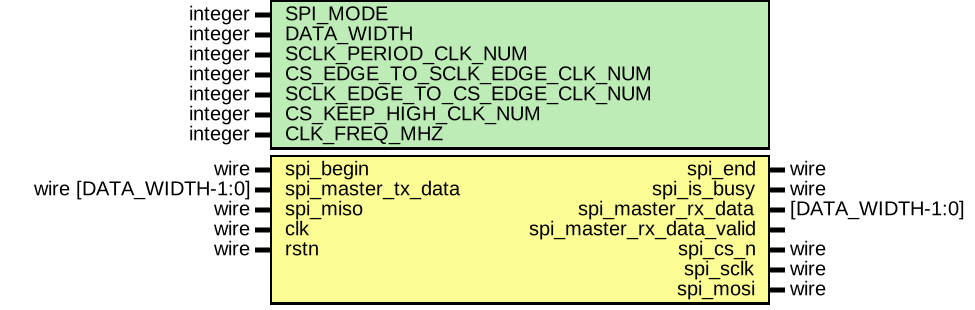
2. Module Block Diagram
3. Signal Interfaces
3.1 Parameter List
| Parameter Name | Type | Default Value | Description |
|---|---|---|---|
| SPI_MODE | integer | 3 | SPI mode, options are 0, 1, 2, 3 (default) |
| DATA_WIDTH | integer | 16 | Bit width of data sent or received in a single communication, minimum is 2, common values are 8/16 |
| SCLK_PERIOD_CLK_NUM | integer | 4 | fSCLK, number of CLK cycles corresponding to SCLK period, must be even, minimum is 2 |
| CS_EDGE_TO_SCLK_EDGE_CLK_NUM | integer | 1 | TCC, number of CLK cycles from CS_N falling edge to the first SCLK edge, minimum is 1 |
| SCLK_EDGE_TO_CS_EDGE_CLK_NUM | integer | 3 | TCCH, number of CLK cycles from the last SCLK edge to CS_N rising edge, minimum is 3 |
| CS_KEEP_HIGH_CLK_NUM | integer | 2 | TCWH, number of CLK cycles to keep CS_N high after going low, minimum is 2 |
| CLK_FREQ_MHZ | integer | 100 | Module operating clock, commonly 100/120 |
3.2 Interface Signal List
| Signal Group | Signal Name | Direction | Description |
|---|---|---|---|
| External Control SPI Signals | spi_begin | input | Start a single SPI communication, active high, only effective when spi_is_busy is low |
| spi_end | output | End a single SPI communication, active high, lasts only one clock cycle | |
| spi_is_busy | output | Indicates SPI busy status, high level indicates SPI is working | |
| spi_master_tx_data[DATA_WIDTH-1:0] | input | Data to be sent via SPI, data is always sent with the highest bit first | |
| spi_master_rx_data[DATA_WIDTH-1:0] | output | Data received via SPI, the first data read is the highest bit | |
| spi_master_rx_data_valid | output | Indicates valid received data, active high | |
| SPI Hardwired Connections | spi_cs_n | output | Chip select, active low |
| spi_sclk | output | SPI clock, provided by the master | |
| spi_mosi | output | Master output, slave input | |
| spi_miso | input | Master input, slave output | |
| Clock and Reset | clk | input | Module operating clock |
| rstn | input | Module reset, active low |
4. Coding Concepts
-
Control SPI mode, data bit width, clock frequency, and three timing parameters through parameters
parameter integer SPI_MODE                     = 3,  // SPI mode, options are 0, 1, 2, 3 (default)
parameter integer DATA_WIDTH                   = 16, // Bit width of data sent or received in a single communication, minimum is 2, common values are 8/16
parameter integer SCLK_PERIOD_CLK_NUM          = 4,  // fSCLK, number of CLK cycles corresponding to SCLK period, must be even, minimum is 2
parameter integer CS_EDGE_TO_SCLK_EDGE_CLK_NUM = 1,  // TCC, number of CLK cycles from CS_N falling edge to the first SCLK edge, minimum is 1
parameter integer SCLK_EDGE_TO_CS_EDGE_CLK_NUM = 3,  // TCCH, number of CLK cycles from the last SCLK edge to CS_N rising edge, minimum is 3
parameter integer CS_KEEP_HIGH_CLK_NUM         = 2,  // TCWH, number of CLK cycles to keep CS_N high after going low, minimum is 2
parameter integer CLK_FREQ_MHZ                 = 100 // Module operating clock, commonly 100/120
Note that the delays here are not real values, but relative values in terms of the module clock CLK, and due to the limitations of the three-stage state machine output timing logic, the delay parameters cannot be zero and have minimum value restrictions. This does not affect practical applications, as these parameters cannot be zero in actual applications, and even if the delay is slightly longer (e.g., TCCH=30ns), it can still work normally.
-
Perform validity checks on parameters to restrict parameter assignments
//++ Parameter Validity Check ++++++++++++++++++++++++++++++++++++++++++++++++++++++++++++ initialbegin if (SPI_MODE != 0 && SPI_MODE != 1 && SPI_MODE != 2 && SPI_MODE != 3) $error("SPI_MODE must be 0, 1, 2, 3"); if (DATA_WIDTH < 2) $error("DATA_WIDTH must be >= 2"); if (SCLK_PERIOD_CLK_NUM < 2 || (SCLK_PERIOD_CLK_NUM % 2 != 0)) $error("SCLK_PERIOD_CLK_NUM must be even and >= 2"); if (CS_EDGE_TO_SCLK_EDGE_CLK_NUM < 1) $error("CS_EDGE_TO_SCLK_EDGE_CLK_NUM must be >= 1"); if (SCLK_EDGE_TO_CS_EDGE_CLK_NUM < 3) $error("SCLK_EDGE_TO_CS_EDGE_CLK_NUM must be >= 3"); if (CS_KEEP_HIGH_CLK_NUM < 2) $error("CS_KEEP_HIGH_CLK_NUM must be >= 2"); end //-- Parameter Validity Check ------------------------------------------------------------ -
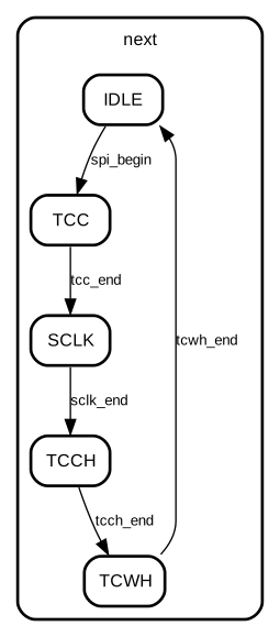
Use a three-stage state machine to control the entire SPI transmission process, as shown in the diagram below
5. Usage Instructions
// External Control SPI Signals
input  wire spi_begin,   // Start a single SPI communication, active high, only effective when spi_is_busy is low
output wire spi_end,     // End a single SPI communication, active high, lasts only one clock cycle
output wire spi_is_busy, // Indicates SPI busy status, high level indicates SPI is working
input  wire [DATA_WIDTH-1:0] spi_master_tx_data, // Data to be sent via SPI, data is always sent with the highest bit first
output reg  [DATA_WIDTH-1:0] spi_master_rx_data, // Data received via SPI, the first data read is the highest bit
output reg                   spi_master_rx_data_valid, // Indicates valid received data, active high
The external module controls SPI read and write through the above signals, with the following explanations:
-
When spi_is_busy is high, this SPI master module does not respond to any external signals. Therefore, the external module needs to monitor the spi_is_busy signal, and when it is low, send spi_begin to start SPI control
-
The SPI master module will latch spi_master_tx_data as the data to be sent when spi_begin is high and spi_is_busy is low
This interface is basically consistent with the AXI Stream interface usage.
6. Simulation Verification
See this series of articles – Verilog Functional Module – SPI Master and Slave (04) – SPI Master-Slave Loopback Simulation and Testing.
7. Source Code Sharing
The source code is open source on Gitee and Github, synchronized on both platforms:
Gitee: [Verilog Functional Module – SPI Master and Slave](https://gitee.com/xuxiaokang/verilog-function-module–SPI-Master-Slave)
Github: [zhengzhideakang/Verilog–SPI-Master-Slave](https://github.com/zhengzhideakang/Verilog–SPI-Master-Slave)
If this article has been helpful to you, feel free to like, share, bookmark, and comment to let more people see it. Your support is greatly appreciated.
If you have any questions about the article content, please be sure to describe the issue clearly, leave a comment or message me, and I will respond when I see it.

Xu Xiaokang’s Blogcontinues to share high-quality hardware, FPGA, and embedded knowledge, software, tools, and more. Everyone is welcome to follow.