Introduction
The NXP “FRDM-MCXN947” evaluation activity is co-hosted by Avnet and Eefocus. This content is published by Eefocus users and has been authorized for reproduction. The original article can be viewed in the Eefocus engineer community.
TFT LCD Module Introduction
The module is named SPI_Module_MSP3323, with a driver chip of ILI9341, and a screen size of 240×320 pixels, featuring built-in GRAM. It can be driven via a 4-wire SPI, allowing for data and command transmission as well as reading IC parameters and even pixel colors from the screen.
Module Back
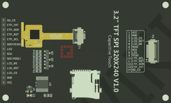
Module Pins
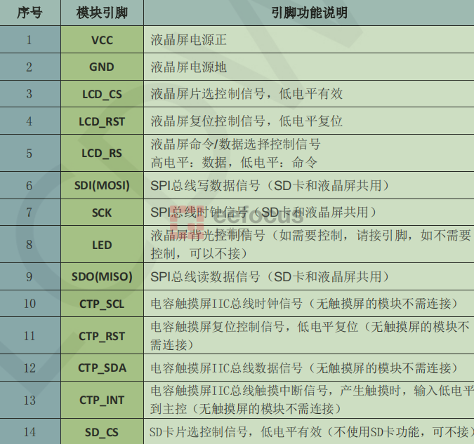
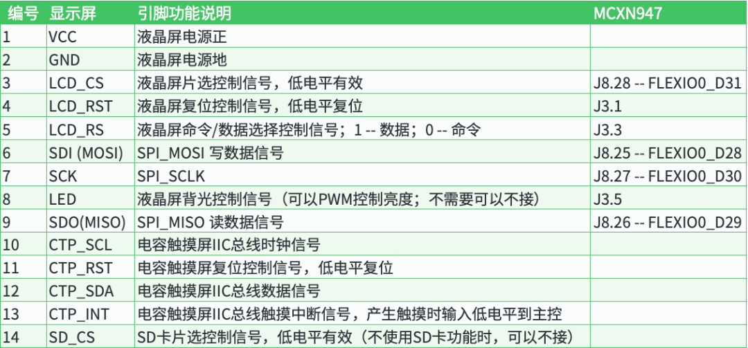
MCXN947 Interface
Currently, only the display interface has been ported, focusing solely on the pins related to the display.
The MCXN947 drives the TFT LCD using a 4-wire SPI, selecting the FLEXIO_SPI_EDMA method for driving. The relevant pins for FLEXIO_SPI are as follows: FLEXIO_Dxx.
Introduction to FLEXIO
The MCXN947 has only one FLEXIO module, which is FLEXIO0.FLEXIO is a highly configurable module that provides:
-
Simulation of various serial or parallel communication protocols;
-
Flexible 16-bit timers supporting various trigger, reset, enable, and disable conditions;
-
Programmable logic blocks allowing for on-chip digital logic functions and configurable interactions between internal and external modules;
-
Programmable state machines to offload basic system control functions from the CPU;
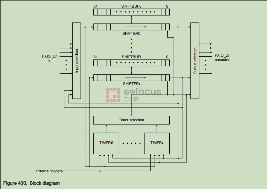
FLEXIO Block Diagram
The following diagram provides a high-level overview of the FLEXIO timer and shifter register configuration.
FLEXIO uses shifters, timers, and external triggers to move data into or out of FLEXIO. As shown in the block diagram, the timer controls the timing of this data shifting, and you can configure the timer to use general timer functions, external triggers, or various other conditions to determine control logic.
FLEXIO Features
1. A 32-bit shifter register array with transmission, reception, data matching, logic, and state modes:
-
Supports double-buffered shifting operations for continuous data transmission;
-
Supports shifter connections for large block data transmission;
-
Supports automatic start and stop bit generation;
-
Parallel interface support for multiple shift widths of 1, 2, 4, 8, 16, or 32 bits;
-
Interrupt, DMA, or polling for transmission and reception operations;
2. Highly flexible 16-bit timers supporting various internal or external triggers, resets, enables, and disables:
-
Programmable baud rate independent of bus clock frequency, supporting asynchronous operation in stop mode devices;
-
Programmable logic modes for integrating external digital logic functions or combining pins, shifters, or timer functions to produce complex outputs;
-
Programmable state machines to offload basic system control functions from the CPU, supporting up to 8 states, 8 outputs, and 3 optional inputs for each state;
3. Integrated general-purpose I/O registers and edge interrupts on pin rising or falling edges to simplify software support;
4. Supports a wide range of protocols, including but not limited to: I2C, SPI, I2S, Camera IF, Motorola 68K or Intel 8080 bus, PWM waveform generation, input capture (pulse edge interval measurement), such as SENT
Pin Configuration
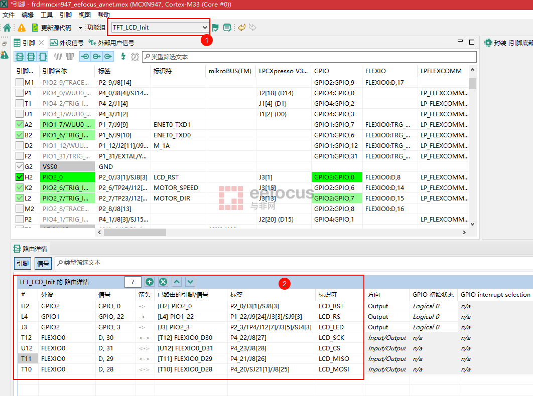
Currently, to light up the LCD, only the display-related pins need to be configured, as shown in the following diagram:
-
Create a function group in MCUXpress Config Tools named TFT_LCD_Init,
-
Set the pin routing information and modify the identifiers for each pin;
-
Among them, LCD_RST, LCD_RS, LCD_LED are all GPIO Outputs, corresponding to J3.1, J3.3, J3.5.
-
The SPI pins simulated by FLEXIO are J8.27, J8.28, J8.26, J8.25.
Porting
01
Porting Approach
The SPI interface driving the TFT LCD mainly involves the output of 3 control pins, sending and reading 8-bit data via SPI.
02
3 GPIO Control Pins
All initialized as GPIO OUTPUT.
-
Among them, LCD_LED is the backlight pin, pulling high lights the screen, pulling low turns it off. Currently, it only needs to output a high level during initialization;
-
Among them, LCD_RS is the data/command selection function, requiring the pin level setting function, which can be provided with two macro definitions;
-
Among them, LCD_RST is the LCD reset pin, outputting low indicates reset, which can be provided with two macro definitions;
03
SPI Pins
Initialize the 4 pins of FLEXIO0, then initialize FLEXIO_SPI and associate these 4 pins.
Key Code
01
GPIO Control Pins
The following port_LCD_CtrlPin_Init() function is newly added, simply setting LCD_LED to output high, as the initialization of these 3 pins has already been configured by MCUXpresso Config Tools and generated initialization code, see the following TFT_LCD_Init() function.
(Swipe to view)
/** * @brief LCD control pin initialization * LCD_RST --> J3.1 P2_0 Reset pin: low level reset * LCD_RS --> J3.3 P1_22 Command data selection pin: high level--data; low level--command * LCD_LED --> J3.5 P2_3 Backlight pin: high level lights up, can also PWM adjust brightness * * @param */void port_LCD_CtrlPin_Init(void){// These 3 pins have been initialized in BOARD_InitBootPins() LCD_LED(1);}(Swipe to view)
/* FUNCTION ************************************************************************************************************ * * Function Name : TFT_LCD_Init * Description : Configures pin routing and optionally pin electrical features. * * END ****************************************************************************************************************/void TFT_LCD_Init(void){ /* Enables the clock for GPIO1: Enables clock */ CLOCK_EnableClock(kCLOCK_Gpio1); /* Enables the clock for GPIO2: Enables clock */ CLOCK_EnableClock(kCLOCK_Gpio2); /* Enables the clock for PORT1: Enables clock */ CLOCK_EnableClock(kCLOCK_Port1); /* Enables the clock for PORT2: Enables clock */ CLOCK_EnableClock(kCLOCK_Port2); /* Enables the clock for PORT4: Enables clock */ CLOCK_EnableClock(kCLOCK_Port4); gpio_pin_config_t LCD_RS_config= { .pinDirection = kGPIO_DigitalOutput, .outputLogic = 0U }; /* Initialize GPIO functionality on pin PIO1_22 (pin L4) */ GPIO_PinInit(TFT_LCD_LCD_RS_GPIO, TFT_LCD_LCD_RS_PIN, &LCD_RS_config); gpio_pin_config_t LCD_RST_config= { .pinDirection = kGPIO_DigitalOutput, .outputLogic = 0U }; /* Initialize GPIO functionality on pin PIO2_0 (pin H2) */ GPIO_PinInit(TFT_LCD_LCD_RST_GPIO, TFT_LCD_LCD_RST_PIN, &LCD_RST_config); gpio_pin_config_t LCD_LED_config= { .pinDirection = kGPIO_DigitalOutput, .outputLogic = 0U }; /* Initialize GPIO functionality on pin PIO2_3 (pin J3) */ GPIO_PinInit(TFT_LCD_LCD_LED_GPIO, TFT_LCD_LCD_LED_PIN, &LCD_LED_config); /* PORT1_22 (pin L4) is configured as PIO1_22 */ PORT_SetPinMux(TFT_LCD_LCD_RS_PORT, TFT_LCD_LCD_RS_PIN, kPORT_MuxAlt0); PORT1->PCR[22] = ((PORT1->PCR[22] & /* Mask bits to zero which are setting */ (~(PORT_PCR_DSE_MASK|PORT_PCR_IBE_MASK))) /* Drive Strength Enable: High. */ |PORT_PCR_DSE(PCR_DSE_dse1) /* Input Buffer Enable: Enables. */ |PORT_PCR_IBE(PCR_IBE_ibe1)); /* PORT2_0 (pin H2) is configured as PIO2_0 */ PORT_SetPinMux(TFT_LCD_LCD_RST_PORT, TFT_LCD_LCD_RST_PIN, kPORT_MuxAlt0); PORT2->PCR[0] = ((PORT2->PCR[0] & /* Mask bits to zero which are setting */ (~(PORT_PCR_DSE_MASK|PORT_PCR_IBE_MASK))) /* Drive Strength Enable: High. */ |PORT_PCR_DSE(PCR_DSE_dse1) /* Input Buffer Enable: Enables. */ |PORT_PCR_IBE(PCR_IBE_ibe1)); /* PORT2_3 (pin J3) is configured as PIO2_3 */ PORT_SetPinMux(TFT_LCD_LCD_LED_PORT, TFT_LCD_LCD_LED_PIN, kPORT_MuxAlt0); PORT2->PCR[3] = ((PORT2->PCR[3] & /* Mask bits to zero which are setting */ (~(PORT_PCR_DSE_MASK|PORT_PCR_IBE_MASK))) /* Drive Strength Enable: High. */ |PORT_PCR_DSE(PCR_DSE_dse1) /* Input Buffer Enable: Enables. */ |PORT_PCR_IBE(PCR_IBE_ibe1)); /* PORT4_20 (pin T10) is configured as FLEXIO0_D28 */ PORT_SetPinMux(TFT_LCD_LCD_MOSI_PORT, TFT_LCD_LCD_MOSI_PIN, kPORT_MuxAlt6); PORT4->PCR[20] = ((PORT4->PCR[20] & /* Mask bits to zero which are setting */ (~(PORT_PCR_DSE_MASK|PORT_PCR_IBE_MASK))) /* Drive Strength Enable: High. */ |PORT_PCR_DSE(PCR_DSE_dse1) /* Input Buffer Enable: Enables. */ |PORT_PCR_IBE(PCR_IBE_ibe1)); /* PORT4_21 (pin T11) is configured as FLEXIO0_D29 */ PORT_SetPinMux(TFT_LCD_LCD_MISO_PORT, TFT_LCD_LCD_MISO_PIN, kPORT_MuxAlt6); PORT4->PCR[21] = ((PORT4->PCR[21] & /* Mask bits to zero which are setting */ (~(PORT_PCR_DSE_MASK|PORT_PCR_IBE_MASK))) /* Drive Strength Enable: High. */ |PORT_PCR_DSE(PCR_DSE_dse1) /* Input Buffer Enable: Enables. */ |PORT_PCR_IBE(PCR_IBE_ibe1)); /* PORT4_22 (pin T12) is configured as FLEXIO0_D30 */ PORT_SetPinMux(TFT_LCD_LCD_SCK_PORT, TFT_LCD_LCD_SCK_PIN, kPORT_MuxAlt6); PORT4->PCR[22] = ((PORT4->PCR[22] & /* Mask bits to zero which are setting */ (~(PORT_PCR_DSE_MASK|PORT_PCR_IBE_MASK))) /* Drive Strength Enable: High. */ |PORT_PCR_DSE(PCR_DSE_dse1) /* Input Buffer Enable: Enables. */ |PORT_PCR_IBE(PCR_IBE_ibe1)); /* PORT4_23 (pin U12) is configured as FLEXIO0_D31 */ PORT_SetPinMux(TFT_LCD_LCD_CS_PORT, TFT_LCD_LCD_CS_PIN, kPORT_MuxAlt6); PORT4->PCR[23] = ((PORT4->PCR[23] & /* Mask bits to zero which are setting */ (~(PORT_PCR_DSE_MASK|PORT_PCR_IBE_MASK))) /* Drive Strength Enable: High. */ |PORT_PCR_DSE(PCR_DSE_dse1) /* Input Buffer Enable: Enables. */ |PORT_PCR_IBE(PCR_IBE_ibe1));}And provide macro definitions to implement the GPIO pin output high and low level functions:
(Swipe to view)
// Hardware CS, ignored here#define LCD_CS_SET#define LCD_CS_CLR// Data, command selection#define LCD_RS_SETGPIO_PinWrite(TFT_LCD_LCD_RS_GPIO, TFT_LCD_LCD_RS_GPIO_PIN, 1)#define LCD_RS_CLRGPIO_PinWrite(TFT_LCD_LCD_RS_GPIO, TFT_LCD_LCD_RS_GPIO_PIN, 0)#define LCD_RST_SETGPIO_PinWrite(TFT_LCD_LCD_RST_GPIO, TFT_LCD_LCD_RST_GPIO_PIN, 1)#define LCD_RST_CLRGPIO_PinWrite(TFT_LCD_LCD_RST_GPIO, TFT_LCD_LCD_RST_GPIO_PIN, 0)02
FLEXIO_SPI Initialization
The corresponding pin routing has been configured in TFT_LCD_Init(), here we only need to initialize FLEXIO_SPI and associate the corresponding 4 pins.
03
Global Macro Definitions and Variables
(Swipe to view)
/******************************************************************************* * Definitions ******************************************************************************/#define BOARD_FLEXIO_BASE (FLEXIO0)#define FLEXIO_SPI_MOSI_PIN 28U#define FLEXIO_SPI_MISO_PIN 29U#define FLEXIO_SPI_SCK_PIN 30U#define FLEXIO_SPI_CSn_PIN 31U#define FLEXIO_CLOCK_FREQUENCYCLOCK_GetFlexioClkFreq()#define EXAMPLE_FLEXIO_SPI_DMA_BASEADDRDMA0#define FLEXIO_SPI_TX_DMA_CHANNEL (0U)#define FLEXIO_SPI_RX_DMA_CHANNEL (1U)#define FLEXIO_TX_SHIFTER_INDEX 0U#define FLEXIO_RX_SHIFTER_INDEX 2U#define EXAMPLE_TX_DMA_SOURCE kDma0RequestMuxFlexIO0ShiftRegister0Request#define EXAMPLE_RX_DMA_SOURCE kDma0RequestMuxFlexIO0ShiftRegister2Request#define FLEXIO_SPI_BAUD_HIGH (1000000*25)#define FLEXIO_SPI_BAUD_LOW (1000000*1)/******************************************************************************* * Variables ******************************************************************************/static flexio_spi_master_edma_handle_t g_spiHandle;static edma_handle_t txHandle;static edma_handle_t rxHandle;FLEXIO_SPI_Type spiDev;flexio_spi_master_config_t userConfig;volatile bool completeFlag =false;static void spi_master_completionCallback(FLEXIO_SPI_Type*base, flexio_spi_master_edma_handle_t *handle, status_t status, void *userData){if (status == kStatus_Success) { completeFlag =true; }}04
FLEXIO_SPI Initialization Function
Initialize FLEXIO_SPI and initialize EDMA.
(Swipe to view)
/** * @brief SPI Initialization * */void port_LCD_SPI_Init(void){ uint8_t i =0; uint8_t err =0; dma_request_source_t dma_request_source_tx; dma_request_source_t dma_request_source_rx; edma_config_t config;/* attach PLL0 to FLEXIO */CLOCK_SetClkDiv(kCLOCK_DivFlexioClk, 1u);CLOCK_AttachClk(kPLL0_to_FLEXIO);/* Init FlexIO SPI. *//* * userConfig.enableMaster = true; * userConfig.enableInDoze = false; * userConfig.enableInDebug = true; * userConfig.enableFastAccess = false; * userConfig.baudRate_Bps = 500000U; * userConfig.phase = kFLEXIO_SPI_ClockPhaseFirstEdge; * userConfig.dataMode = kFLEXIO_SPI_8BitMode; */FLEXIO_SPI_MasterGetDefaultConfig(&userConfig);// NOTE: Modify SPI communication speed here userConfig.baudRate_Bps =FLEXIO_SPI_BAUD_HIGH; spiDev.flexioBase =BOARD_FLEXIO_BASE; spiDev.SDOPinIndex=FLEXIO_SPI_MOSI_PIN; spiDev.SDIPinIndex=FLEXIO_SPI_MISO_PIN; spiDev.SCKPinIndex=FLEXIO_SPI_SCK_PIN; spiDev.CSnPinIndex=FLEXIO_SPI_CSn_PIN; spiDev.shifterIndex[0] =FLEXIO_TX_SHIFTER_INDEX; spiDev.shifterIndex[1] =FLEXIO_RX_SHIFTER_INDEX; spiDev.timerIndex[0] = 0U; spiDev.timerIndex[1] = 1U; dma_request_source_tx = (dma_request_source_t)EXAMPLE_TX_DMA_SOURCE; dma_request_source_rx = (dma_request_source_t)EXAMPLE_RX_DMA_SOURCE;#if defined(FSL_FEATURE_SOC_DMAMUX_COUNT) &&FSL_FEATURE_SOC_DMAMUX_COUNT/*Init EDMA for example.*/DMAMUX_Init(EXAMPLE_FLEXIO_SPI_DMAMUX_BASEADDR);/* Request DMA channels for TX & RX. */DMAMUX_SetSource(EXAMPLE_FLEXIO_SPI_DMAMUX_BASEADDR, FLEXIO_SPI_TX_DMA_CHANNEL, dma_request_source_tx);DMAMUX_SetSource(EXAMPLE_FLEXIO_SPI_DMAMUX_BASEADDR, FLEXIO_SPI_RX_DMA_CHANNEL, dma_request_source_rx);DMAMUX_EnableChannel(EXAMPLE_FLEXIO_SPI_DMAMUX_BASEADDR, FLEXIO_SPI_TX_DMA_CHANNEL);DMAMUX_EnableChannel(EXAMPLE_FLEXIO_SPI_DMAMUX_BASEADDR, FLEXIO_SPI_RX_DMA_CHANNEL);#endifEDMA_GetDefaultConfig(&config);EDMA_Init(EXAMPLE_FLEXIO_SPI_DMA_BASEADDR, &config);EDMA_CreateHandle(&txHandle, EXAMPLE_FLEXIO_SPI_DMA_BASEADDR, FLEXIO_SPI_TX_DMA_CHANNEL);EDMA_CreateHandle(&rxHandle, EXAMPLE_FLEXIO_SPI_DMA_BASEADDR, FLEXIO_SPI_RX_DMA_CHANNEL);#if defined(FSL_FEATURE_EDMA_HAS_CHANNEL_MUX) &&FSL_FEATURE_EDMA_HAS_CHANNEL_MUXEDMA_SetChannelMux(EXAMPLE_FLEXIO_SPI_DMA_BASEADDR, FLEXIO_SPI_TX_DMA_CHANNEL, dma_request_source_tx);EDMA_SetChannelMux(EXAMPLE_FLEXIO_SPI_DMA_BASEADDR, FLEXIO_SPI_RX_DMA_CHANNEL, dma_request_source_rx);#endifFLEXIO_SPI_MasterInit(&spiDev, &userConfig, FLEXIO_CLOCK_FREQUENCY);}05
SPI Transmission Function
This only implements a single byte send and receive function, using eDMA interrupts to determine if the transmission is complete.
(Swipe to view)
uint8_t port_LCD_SPI_TxByte(uint8_t data){ flexio_spi_transfer_t xfer = {0}; uint8_t readBack =0;/* Send to slave. */ xfer.txData =&data; xfer.rxData =&readBack; xfer.dataSize =1; xfer.flags = kFLEXIO_SPI_8bitMsb;FLEXIO_SPI_MasterTransferCreateHandleEDMA(&spiDev, &g_spiHandle, spi_master_completionCallback, NULL, &txHandle, &rxHandle);FLEXIO_SPI_MasterTransferEDMA(&spiDev, &g_spiHandle, &xfer);while (!completeFlag); completeFlag =false;return readBack;}06
LCD Read/Write Register and Data Functions
The following are the functions of the LCD abstraction layer, which only need to control the pin output high and low, and SPI transmission of a single byte.
(Swipe to view)
/***************************************************************************** * @name :void LCD_WR_REG(uint8_t data) * @date :2018-08-09 * @function :Write an 8-bit command to the LCD screen * @parameters :data:Command value to be written * @retvalue :None******************************************************************************/void LCD_WR_REG(uint8_t data){ LCD_CS_CLR; LCD_RS_CLR; port_LCD_SPI_TxByte(data); LCD_CS_SET;}/***************************************************************************** * @name :void LCD_WR_DATA(uint8_t data) * @date :2018-08-09 * @function :Write an 8-bit data to the LCD screen * @parameters :data:data value to be written * @retvalue :None******************************************************************************/void LCD_WR_DATA(uint8_t data){ LCD_CS_CLR; LCD_RS_SET; port_LCD_SPI_TxByte(data); LCD_CS_SET;}Execution
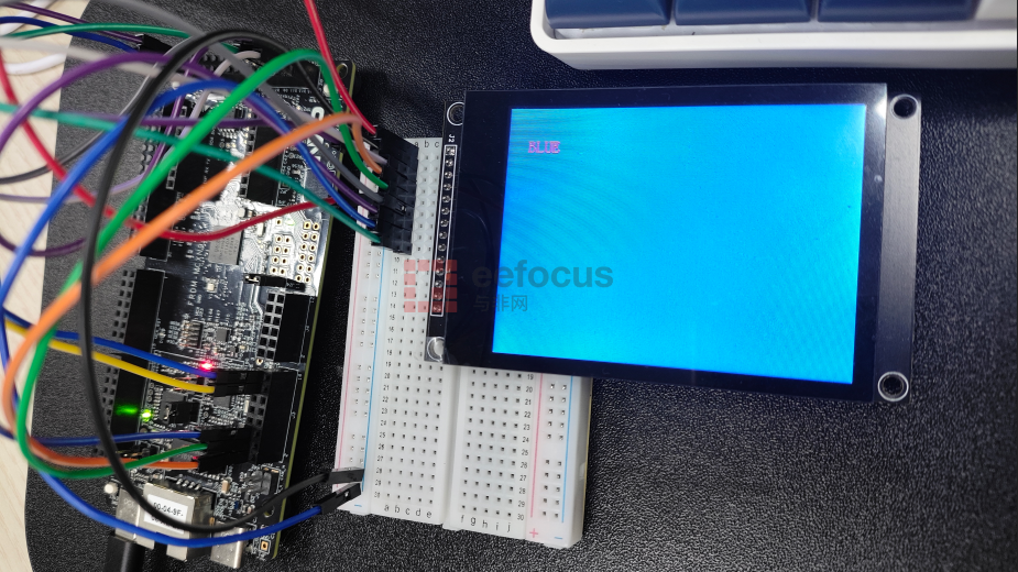
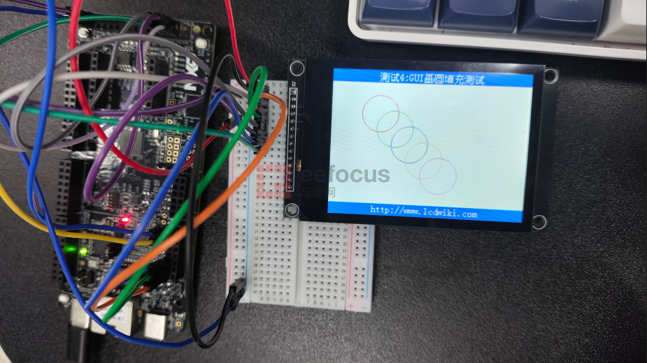
The screen successfully lights up and can display both Chinese and English characters. There were some errors in drawing images, but the refresh speed is very slow. I tried increasing the SPI speed, and tested both debug/release compiler optimization levels, but the screen refresh effect still shows noticeable tearing.
See the demonstration video on Bilibili:
You can click on the end of the article“Read the original article”, to go to the Eefocus engineer community to view the original article.
END
—— More Exciting Content ——


About Avnet
Avnet is a leading global technology distributor and solutions provider, committed to meeting the evolving needs of customers for over a century. Through its specialized and regional business coverage worldwide, Avnet can provide support to customers and suppliers at every stage of the product lifecycle. Avnet helps various types of companies adapt to the changing market environment, accelerating design and supply speed during product development. Avnet is centrally positioned in the entire technology value chain, and this unique position and perspective make it a trusted partner capable of helping customers solve complex design and supply chain challenges, thus achieving revenue faster. To learn more about Avnet, please visit www.avnet.com