I2CIntroduction
I2C (Inter-Integrated Circuit) is a short-distance, low-speed, two-wire serial communication bus introduced by Philips (NXP) in the 1980s. It is widely used in electronic devices due to its simple structure (requiring only the SDA data line and SCL clock line), low wiring costs, and support for multi-master and multi-slave communication. Its main application scenarios cover various fields including consumer electronics, industrial control, automotive electronics, and the Internet of Things.
I2CFeatures
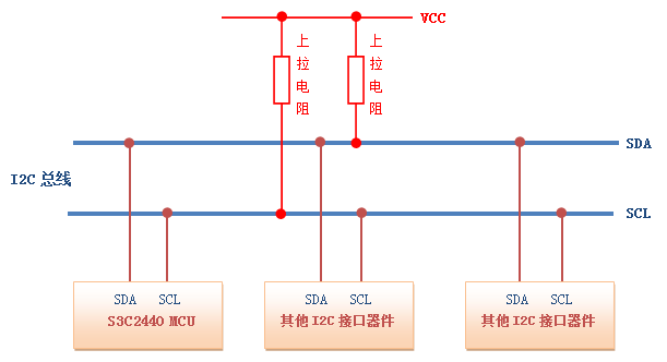
(1))The I2C bus consists of two signals:Serial Data Line (SDA) and Serial Clock Line (SCL), where the data line is used for data transmission and the clock line is used for synchronizing data transmission (i.e., synchronous transmission).
(2)I2C supports bidirectional data exchange. Since there is only one data line, communication ishalf-duplex.
(3)4)The I2C bus operates withopen-drain output, and both the SDA and SCL lines require pull-up resistors. When the bus is idle, both lines are at a high level.
(4)5) The I2C communication bus supportsmulti-master and multi-slave configurations. Any device on the bus capable of sending/receiving data can take control of the bus, but only one master can exist at any given time. (Maximum number of masters: unlimited; maximum number of slaves: theoretically 127).
(5)6)The transmission speeds of I2C are as follows:
a.Standard Mode: Standard Mode = 100Kbps
b.Fast Mode: Fast Mode = 400Kbps
c.High Speed Mode: High Speed Mode = 3.4Mbps
d.Ultra Fast Mode: Ultra Fast Mode = 5Mbps
(6) Each device connected to the bus has aunique address, which the master uses to access the slave devices.
(7) When multiple masters use the bus simultaneously, anarbitration method is required to determine which device occupies the bus.
(8)The I2C bus signal levels are typically 5V and 3.3V. If devices on the bus are not compatible with these two levels, level conversion is required.
(9) The actual usage rate of I2C is not high, commonly at 400Kbps, and I2C communication can be simulated using IO ports.
I2CProtocolOverview
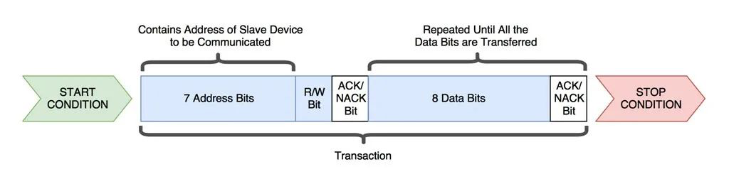
The I2C protocol transmission diagram is shown below. The I2C protocol standard defines two types of frames: Address Frame and Data Frame. The Address Frame is used for the master to specify the target slave device it needs to access; the Data Frame is used to transmit data to the target slave device. A complete I2C protocol consists of idle state, start bit, address bit, read/write flag bit, acknowledgment bit, data bits, stop bit, and repeated start signal. The following two diagrams explain the I2C protocol.
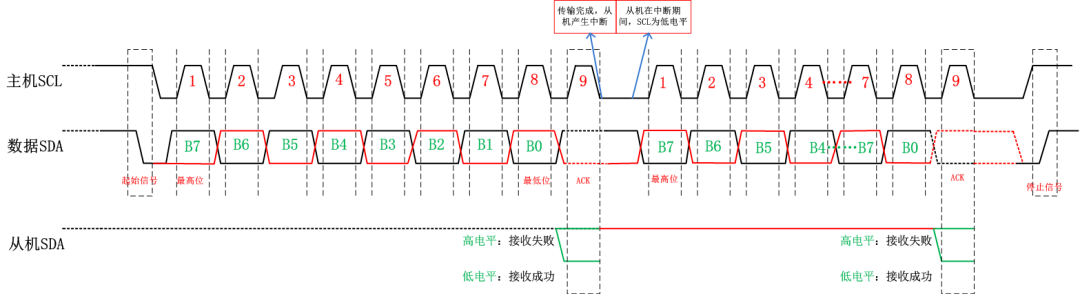
The timing of data transmission is shown in the diagram below:
[Idle State]
In the idle state, due to the open-drain structure of I2C, both SCL and SDA are at a high level.
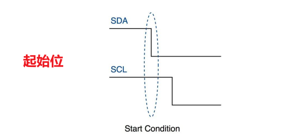
[Start Bit]-Start] When SCL is high, SDA is pulled from high to low (falling edge), marking the start of communication. If two master devices wish to gain control of the bus at the same time, arbitration occurs, and the one that pulls SDA low first wins control of the bus. During the entire communication period, multiple Start signals can exist to initiate each new communication sequence without needing to relinquish control of the bus.
[Address Bit]-Address
I2C has only one data line, making it impossible to specify the target slave device. Therefore, each device connected to the bus must have a unique address for the master to address. Addresses can be in the form of 7+1 or 10+1, where 7+1 refers to a 7-bit address plus a read/write flag bit, supporting up to 128 addresses (0x00~0x7F). 10+1 refers to a 10-bit address plus a read/write flag bit, supporting up to 1024 addresses. The read/write flag occupies 1-bit, where writing 1 indicates a read operation, and writing 0 indicates a write operation. The protocol specifies that the address bits are sent starting from the most significant bit (MSB) to the least significant bit (LSB).
As mentioned above, I2C supports 10-bit device addresses, which require two frames to transmit the address of the slave device. The first frame’s first 5 bits are fixed as b11110, followed by the high 2 bits of the slave device address. The 8th bit remains the R/W bit, followed by an ACK bit, and then another 8 bits of the address. After sending, the slave device will respond.
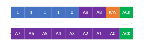
[Acknowledgment Bit]-ACK/NACK] After the master device sends the address frame, it relinquishes control of the SDA bus to allow the slave device to take control. At this point, the slave device should respond with an ACK before the 9th clock pulse (by pulling SDA low, indicating successful reception). If the slave device does not pull SDA low, it indicates that the slave may not have received the data. In this case, the master device decides whether to send a Stop or Repeated Start Condition.
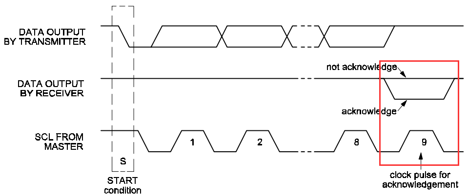
ACK/NACK Explanation:
(1) ACK Signal: Timing of transmission (after each byte transmission, the receiver must send an ACK signal). Generation method (the receiver pulls the SDA line low during the ACK clock pulse, indicating successful data reception). Function (to inform the sender that the data has been successfully received and to request the transmission of the next byte).
(2) NACK Signal: Timing of transmission (only when the master reads data, the master device sends a NACK signal to inform the slave device to stop sending). Generation method (the receiver keeps SDA high during the ACK clock pulse, indicating refusal to receive more data). Function: to end the current data transmission; the slave will stop operation and release the bus after receiving NACK.
[Data Bit]-Data] Each byte transmitted on SDA must be 8 bits, and there is no limit to the number of bytes that can be sent in each transmission. Each byte must be followed by an acknowledgment bit (ACK or NACK) until a stop condition is generated. The master device is responsible for generating the clock and must prepare the data before the clock rises. The protocol specifies that the data bits are sent starting from the most significant bit (MSB) to the least significant bit (LSB).
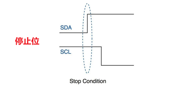
[Stop Bit]-Stop] When all data has been sent, the master device must generate a stop signal to inform the slave device that data transmission is complete. When SCL is high, SDA is pulled from low to high (rising edge), marking the end of communication.
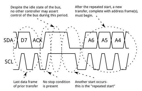
[Repeated Start Signal]-Repeated Start Condition] The master device can initiate multiple start signals to complete data transmission. As long as a stop signal is not sent, other master devices on the bus cannot take control. Sometimes, after sending a set of data, the master may wish to resend data, hence the repeated start signal. The repeated start signal occurs when SCL is high, and SDA transitions from high to low, generating a falling edge of SDA during the high level of SCL.
I2CRead/Write Operations
[Write Operation]
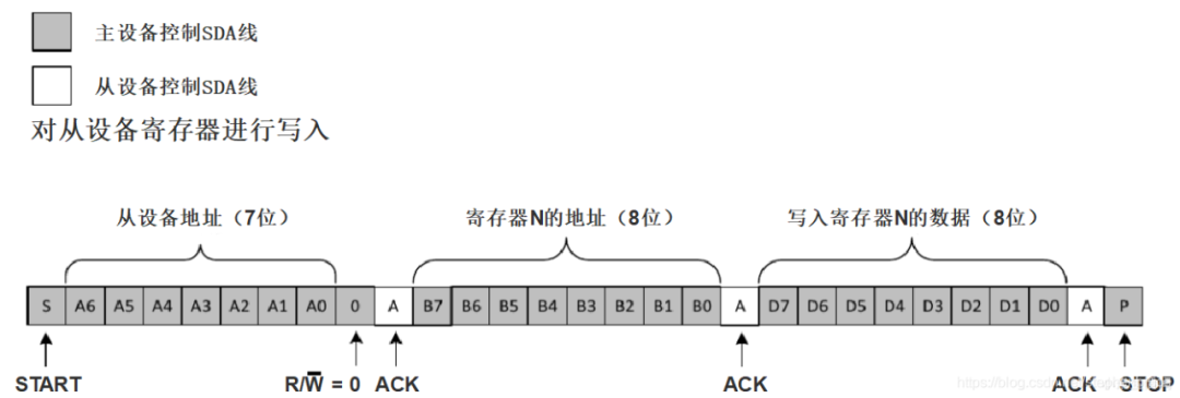
As shown in the diagram below, when the master device writes data to the slave device via the I2C bus, the master first sends a start condition with the slave device address and sets the read/write flag to 0 (R/W bit, where 0 indicates writing). After the slave device sends an acknowledgment bit, the master sends the register address of the register it wishes to write to (8 bits). After the slave device confirms with an acknowledgment bit, the master sends data to the slave device’s register until all desired data has been sent. The master then terminates the transmission with a Stop condition.
[Read Operation]
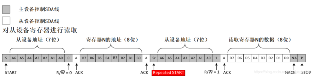
As shown in the diagram below, when the master device reads data from the slave device via the I2C bus, the master must first indicate which register it wishes to read from. The master starts the transmission similarly to writing, by sending the R/W bit as 0 (indicating writing) and the register address from which it wishes to read. Once the slave device confirms the register address, the master sends a start condition with the slave device address and sets the R/W bit to 1 (indicating reading). The slave device will confirm the read request, and the master will release the SDA bus but continue to send clock pulses. At the end of each data byte, the master will send an ACK to let the slave know it is ready to receive more data. Once the master has received the expected number of bytes, it will send a NACK, indicating that reading is complete and no further ACK signal is needed from the slave. The master will then end the communication with a Stop condition.
I2CPull-Up Resistor Value CalculationUsage
[Function of Pull-Up Resistors]
I2C bus SDA and SCL pins typically use open-drain output or open-collector structure. This structure allows devices to actively pull the bus low (by turning on internal MOSFETs or transistors) but not actively output high (no active pull-up circuit in the output stage). Without external pull-up resistors, the bus will be in a floating state (high impedance) when not pulled low, leading to unstable levels (which may fluctuate randomly due to interference), making it impossible for devices to determine the bus state.
The function of the pull-up resistor is to ensure that when all devices are not pulling the bus low, the bus is “passively pulled high” to a high level through an external power source (such as 3.3V or 5V) via the resistor, ensuring a stable high level in the idle state.
[Pull-Up Resistor Calculation]
I2C commonly uses pull-up resistors of 2K or 4.7K. If the pull-up resistor value is too small, the current (Ic) flowing into VCC will increase, causing the MOSFET (or transistor) to not fully turn on (Ib x β < Ic), changing from saturation to amplification state, which will increase the low-level output value. If the pull-up resistor is too large, the bus capacitance will cause the RC time constant to be too large, resulting in slow rising edges, which may severely affect data sampling and lead to transmission errors.
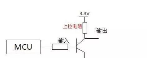
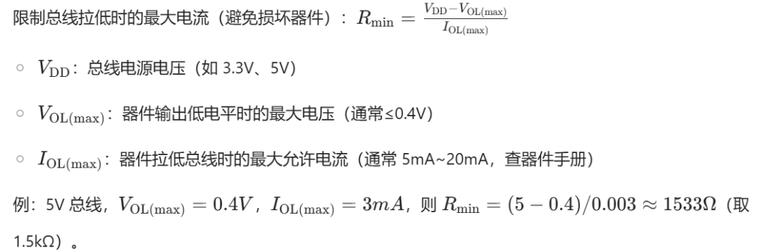
(1) Minimum Pull-Up Resistor Value
(2) Maximum Pull-Up Resistor Value
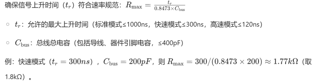
In summary:The power supply voltage limits the minimum value of the pull-up resistor; the load capacitance (bus capacitance) limits the maximum value of the pull-up resistor.
[Practical Application Principles]
(1) The resistor value should be between Rmin and Rmax, with a typical value of 4.7kΩ (suitable for most 3.3V/5V, standard/fast mode scenarios).
(2) High-speed mode (3.4Mbps) requires smaller resistors (such as 1kΩ~2kΩ) to avoid slow rising times.
(3) When the bus capacitance is large (close to 400pF), the resistor value should be reduced to speed up the rising time.
(4) In multi-node scenarios, 2-3 identical resistors can be connected in parallel (e.g., two 4.7kΩ in parallel ≈ 2.35kΩ) to balance current and rising time.
I2CCommon Issues and Solutions
[Communication Anomalies Due to Improper Hardware/Software Design]
(1) Pull-up resistors are too large, causing data sampling errors and communication anomalies.(2) Incorrect address configuration leads to failed access to slave devices, causing communication anomalies.
(3) Communication rate configured too high, causing incompatibility between master and slave devices, leading to communication anomalies.(4) Slave device malfunction, such as power issues or chip faults, leading to communication anomalies.
(5) Simulating I2C with IO ports, incorrect pin configuration or code configuration leads to communication anomalies.
[I2C Deadlock]
In practical use of I2C, one of the most common issues is deadlock, which is mainly manifested as:SCL remains high, and SDA remains low.
Three possible ways to cause I2C deadlock:
(1) A fault in one of the slave devices on the bus pulls SDA low, causing I2C deadlock.(2) The master device repeatedly restarts while the slave device is returning data (e.g., during the slave device response phase or data sending phase), causing SDA to be locked.
(3) Pull-up resistor failure (e.g., open circuit), SDA/SCL lines shorted to ground or power, or physical damage to device pins, causing I2C deadlock.
The solutions to I2C deadlock mainly include two methods:
(1) The master device detects that SDA has been pulled low for an extended period and actively resets or powers off and restarts the slave device to release SDA. However, this method requires the slave device to have a reset pin or power-off restart enable control pin, and the master device must be able to control these two pins.
(2) The master device detects that SDA has been pulled low for an extended period and pushes 9 clock pulses onto the SCL bus, simulating a request for the slave device address, thereby releasing the faulty slave device and allowing SDA to return to high.
If you find this useful, please like, bookmark, and share. If there are any errors in the article, please leave a comment for discussion and correction. The “Hardware Knowledge Base” thanks you!