Source: Semiconductor Think Tank
History of Semiconductor Development
1 Semiconductors are the foundation of information technology.
The invention of large-scale integrated circuits, semiconductor lasers, and various semiconductor devices in the last century played a crucial role in the modern information technology revolution, triggering a new global industrial revolution. Information technology is the major trend in today’s economic and social development, and the level of informatization has become an important indicator of the modernization of a country or region.
Entering the 21st century, the world is accelerating the pace of informatization construction. Driven by the needs of the information technology revolution, semiconductor physics, materials, and devices will undergo new and faster developments. The size of integrated circuits will continue to shrink, leading to the emergence of new quantum effect devices; wide bandgap semiconductors represent a new direction, with broad applications in short-wavelength lasers, white light emitting diodes, and high-frequency high-power devices; nanoelectronic devices may serve as the next generation of semiconductor microelectronics and optoelectronic devices; utilizing single electrons, single photons, and spin devices for quantum control will play a key role in the practical realization of quantum computing and quantum communication.
2 The Invention of Transistors
In 1945, at the end of World War II, the president of Bell Labs, Barclay, decided to establish a solid-state physics group to adapt the lab’s work from wartime to peacetime needs. Shockley was responsible for the semiconductor physics group, which included members like Bardeen, Brattain, Gibney, and Moore. Shockley and Bardeen were theoretical physicists, Brattain was an experimental physicist, Gibney was a physical chemist, and Moore was an electrical engineer. This combination of expertise was a golden match for semiconductor physics research and the invention of transistors, making them efficient and effective. From the start, they focused on the study of semiconductor materials silicon and germanium based on their experiences from the mid-1930s and later considerations.
During World War II, the British used radar to detect German bombers. The core of radar was the vacuum tube, which could amplify weak currents. Shockley had been preparing to create a solid-state device capable of amplifying current to replace vacuum tubes since 1939. In December 1947, Bardeen and Brattain created the world’s first germanium point-contact transistor, which had current amplification capabilities.
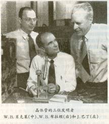
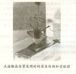
The results of Bardeen and Brattain were published in June 1948. Although the invention of the point-contact transistor opened the door to the development of transistors, its complex structure, poor performance, large size, and manufacturing difficulties limited its promotion and application in the industry, resulting in a weak social impact.
In January 1948, based on his research on p-n junction theory, Shockley invented another type of planar junction transistor and obtained a patent in June 1948. The planar junction transistor, also known as the field-effect transistor, is planar (see Figure 3) and can be mass-produced using some planar processes (such as diffusion, masking, etc.). It was only after the invention of the planar junction transistor that the superiority of transistors was recognized, gradually replacing vacuum tubes.
Due to the contributions of Bardeen, Brattain, and Shockley in the invention of the transistor and junction transistor, they were awarded the Nobel Prize in Physics in 1956. The first application of the semiconductor transistor was the portable radio from Sony, which became a global sensation and made significant profits.
3 The Invention of Integrated Circuits
Transistor radios are much smaller than vacuum tube radios and can be carried around. However, they consist of transistors, resistors, capacitors, and magnetic antennas soldered onto a circuit board, interconnected by wires. Their size is still relatively large, and the assembly process is complex.
In 1958, the U.S. government established a fund for miniaturizing transistor circuits to meet the needs of the U.S. in catching up with the Soviet Union’s launch of the first artificial satellite. At that time, Kilby from Texas Instruments undertook this task, attempting to create a miniaturized circuit that packaged transistors, resistors, and capacitors together. In September 1958, Kilby made the world’s first integrated circuit oscillator, all recorded in his notes from that day. The integrated circuit invented by Kilby obtained patent rights in February 1959, named “miniaturized electronic circuit.”
At the same time, Noyce from Fairchild Semiconductor in California proposed the idea of connecting transistors with aluminum. Five months after Kilby’s invention of the integrated circuit, in February 1959, he used the planar transistor method proposed by Horn to generate an SiO2 mask over the entire silicon wafer, applying photolithography to create windows and lead paths according to a template, and diffusing impurities through the windows to form the base, emitter, and collector, evaporating gold or aluminum to create the integrated circuit. In July 1959, Noyce’s integrated circuit obtained patent rights, named “semiconductor device and lead structure.” From then on, integrated circuits entered a new period of large-scale development.
4 The Invention of Solar Cells
To meet the needs of artificial satellites, in 1954, Pearson and Fuller used phosphorus and boron diffusion technology to create large-area silicon p-n junction solar cells, achieving a photoelectric conversion efficiency of over 6%, exceeding the previous best solar conversion efficiency by 15 times. Its low production cost allows for mass production, leading to rapid large-scale application.
The working principle of solar cells is the photoelectric effect. When light hits the semiconductor, it generates electron-hole pairs within the semiconductor. If an external circuit is connected, current will flow, which is the photoelectric effect.
The commercial application of solar cells began in 1958, when they were selected as the power source for the radio transmitter of the United States’ first artificial satellite, Vanguard I. In the current energy crisis, solar cells have attracted significant attention as a renewable and non-polluting power source.
5 The Invention of Semiconductor Lasers
The working principle of semiconductor light-emitting diodes and lasers is the opposite of solar cells: solar cells generate electricity from light, while light-emitting diodes and lasers generate light from electricity. By injecting current, electrons and holes are introduced into the conduction band and valence band of the semiconductor, respectively. The recombination of electrons and holes produces photons.
In 1962, Hall in the U.S. created the first semiconductor laser using a p-n homojunction (see Figure 8). To generate laser light, three conditions must be met: population inversion, a resonant cavity, and current exceeding a certain threshold.
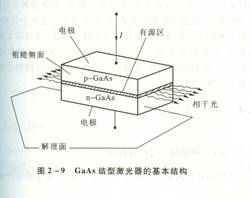
In 1963, Kremer from the U.S. and Alferov from the Soviet Union independently created heterojunction lasers, which used a material with a smaller bandgap width, such as GaAs, in the junction region; the p and n regions on either side used another material with a larger bandgap width, such as AlxGa1-xAs. This way, the light-emitting region is confined to a narrow junction area (see Figure 9). Thus, the light-emitting efficiency was greatly improved, and the threshold current for lasers was reduced. In 1970, the Soviet Union’s Yoffe Institute and the U.S. Bell Labs each created a room-temperature continuous-wave double heterojunction laser, making semiconductor lasers widely used in optical communication.
Due to Kremer and Alferov’s significant contributions to the development of semiconductor lasers, they were awarded the Nobel Prize in Physics in 2000, along with Kilby, the inventor of integrated circuits. The invention of silicon large-scale integrated circuits and semiconductor lasers has ushered the world into an information age based on microelectronics and optoelectronics, greatly promoting social and economic development.
6 The Invention of Molecular Beam Epitaxy Technology
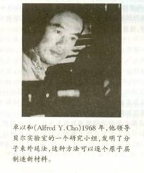
A key technology for manufacturing double heterojunction lasers is molecular beam epitaxy. In 1968, Bell Labs’ Zhuo Yi discovered that by finely controlling the size and time of the beam flow in an ultra-high vacuum chamber, it was possible to grow different layers and types of semiconductor materials as needed, thus inventing molecular beam epitaxy technology. A schematic diagram of the molecular beam epitaxy device is shown in Figure 11. The device operates under ultra-high vacuum conditions (10-10 torr), with a source containing raw material elements (such as Ga, As, Al, etc.) in the evaporation furnace. In front is a controllable shutter; when opened, the evaporated source atoms are directed onto a heated substrate for epitaxial growth. Currently, this technology can achieve the growth of single atomic layers. Surrounding the device are various detection instruments to monitor the growth process.
Applications of Semiconductor Technology
1Large-scale integrated circuits and computers
Large-scale integrated circuits laid the foundation for the development of computers and networks. According to Moore’s Law, the integration of integrated circuits doubles every 18 months, and recently its line width has reached tens of nanometers (millimeters, micrometers, nanometers), with each chip containing hundreds of billions of components. Computer science has reached a high level, with both hardware and software being quite mature, and computers capable of trillions of calculations per second (Tianhe: 20 trillion calculations, second in the world) have emerged, providing powerful tools for various high-speed calculations, massive information processing, and conversion.
Since the birth of computers in 1943, due to the invention of integrated circuits, computers have rapidly developed towards high computing speeds and miniaturization. Currently, major developed countries and China have large-scale computers with over a hundred trillion floating-point operations. China ranks second in the world in manufacturing and owning such supercomputers, second only to the U.S. It can be used for protein analysis, new drug development, and in military applications for simulating nuclear explosions and decoding. It should be noted that China is still lagging in manufacturing the large-scale integrated circuits needed for these computers, with most still needing to be imported.
2Optical Communication Technology
Previously, long-distance communication relied on long-distance telephones or telegrams, which were expensive due to the low number of calls. In 1966, K.C. Kao from the British Standard Communication Laboratory proposed using high-purity, high-transparency glass fibers to transmit laser signals. If its loss could be reduced to 20 decibels per kilometer, long-distance optical communication could be achieved. In 1970, R.D. Maurer and others at the New York Corning Glass Works used a “deposition process” to create dense glass tubes from silicon tetrachloride vapor through flame hydrolysis, which were then heated and drawn into thin glass fibers. The birth of low-loss glass fibers marked a milestone in optical communication technology.
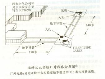
In 1976, Bell Labs conducted the first field experiment of optical communication in Atlanta, achieving good results. The average power loss of the optical fiber was 6 decibels per kilometer, with error-free transmission of information exceeding 10.9 kilometers, equivalent to 17 loops around the optical fiber. In December 1976, Bell Labs announced that optical wave communication had passed its first test, confirming the feasibility of optical wave communication. This marked the arrival of the optical communication era and signaled the formal beginning of the transition from the microelectronics era to the optoelectronics era.
Today, telecommunications networks, computer networks, and cable television networks have become important infrastructures of a country, with all political, economic, military, and scientific activities, as well as people’s daily lives, relying on these three networks. China currently has 850 million telephone users, including 480 million mobile phone users, making it the largest telecommunications network in the world. The number of internet users has reached 137 million, and cable television users have reached 130 million, accounting for one-third of the world.
The future trend is the integration of the three networks. Mobile internet access has become very common, with Apple’s company in the U.S. leading the way in this regard.
Light has different colors and wavelengths. Not all colors of light can propagate in optical fibers.
The losses of optical fibers have their lowest and second-lowest values at 1450-1550 nm and 1250-1350 nm, respectively, making these two bands the main windows for optical fiber communication. To maximize the number of information channels that an optical fiber can transmit, wavelength division multiplexing optical communication systems are used, which divide these two bands into narrow wavelengths, each forming a certain communication capacity. Different wavelength signals are transmitted through a single optical fiber to the other end, and then demultiplexed, allowing the light detector to recover the original electrical signals transmitted at different wavelengths. Since optical signals gradually attenuate during transmission, to achieve long-distance transmission, it is necessary to amplify the signals using erbium-doped fiber amplifiers at regular intervals.
3Wireless Communication Technology (Mobile Phones)
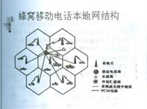
The foundation of wireless communication is the cellular mobile phone system, which was first introduced by Bell Labs in 1978 with the “Advanced Mobile Phone Service” (AMPS) system. This system divides the service area into many small hexagonal geographic areas (cells), resembling a honeycomb (see Figure 19). Each cell contains low-power wireless telephone transmitters, receivers, and a control system, forming a base station. The base stations in different service areas are connected to a central switching entity (mobile phone exchange) via optical fibers, which houses an electronic switching system. The base station network tracks the location of mobile terminals, allowing them to automatically reconnect with adjacent base stations when they move into another cell to continue the call. Since the wireless call power within a cell is low, it only affects a limited area, thus preventing interference with communication signals from other cells.
The first AMPS system successfully tested in Chicago in July 1979. In April 1992, AT&T’s microelectronics group announced the production of integrated circuit chips for the next generation of digital cellular phones, making the company a leading supplier of digital signal processing components for mobile communications. This digital signal processor constituted the DSP1600 series, significantly reducing the size and power of mobile phones, which became very popular in the market.
In addition to mobile phone communication, there are other wireless communication methods (see Figure 20), including satellite transmission of high-definition television, inter-satellite communication, multipoint video communication, wireless local area networks, communication between vehicles, and anti-collision radar, etc. Their working frequencies range from several GHz to 100 GHz.
Various wireless communications and their operating frequencies. The bands range from micrometers to millimeter bands, with frequencies from 20-80 GHz.
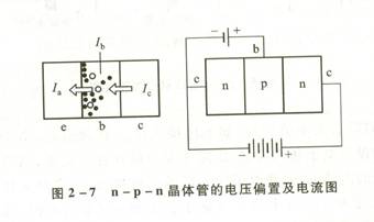
The most critical devices in wireless communications are semiconductor high-frequency oscillators, of which there are currently two types: high electron mobility transistors (HEMT) and heterojunction bipolar transistors (HBT). They are essentially typical transistors, but due to the use of molecular beam epitaxy technology, each layer of the n-p-n structure can be made very thin, reducing the path of electron movement and achieving high cutoff frequencies (fT). Currently, the cutoff frequencies of these two devices have exceeded 100 GHz, meeting the needs of wireless communication.
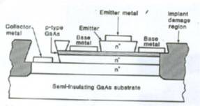
Cross-section of an npn bipolar transistor
4Semiconductor Solar Cells – Silicon Materials for Solar Cells
The silicon materials used for solar cells mainly include: single crystal silicon, amorphous silicon, ribbon silicon, and thin-film polycrystalline silicon. The efficiencies of solar cells made from these materials in laboratories and industries are shown in Figure 22.
Currently, cast polycrystalline silicon accounts for 47.54% of solar cell materials, making it the most significant solar cell material. By 2004, the market share of cast polycrystalline silicon had exceeded 53%. Single crystal silicon accounts for 35.17%, ranking second, while amorphous silicon thin films account for 8.3%, ranking third, and compound semiconductors CuInSe and CdTe account for only 0.6%.
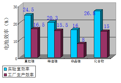
Efficiency of solar cells made from different semiconductor materials in laboratories and industries
5Semiconductor Solar Cells – Polycrystalline Silicon Solar Cells
Until the 1990s, the solar photovoltaic industry was primarily based on single crystal silicon. Although the cost of single crystal silicon batteries has been continuously decreasing, they still lack competitiveness compared to conventional electricity. Therefore, continuously reducing costs is the goal pursued by the photovoltaic community. Since the invention and application of cast polycrystalline silicon in the 1980s, it has seen rapid growth. It has continuously captured the market share of single crystal silicon due to its relatively low cost and high efficiency, and by the beginning of this century, it had accounted for over 50%, becoming the most competitive solar cell material.
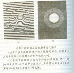
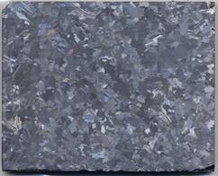
Optical image of the surface of cast polycrystalline silicon wafers
To date, the weight of cast polycrystalline silicon ingots has reached 300 kg, and the size of solar cells has reached 210×210 mm2. By the beginning of this century, the efficiency of polycrystalline silicon solar cells reached 20.3%. In actual production, the highest efficiency of cast polycrystalline silicon solar cells has also reached around 17.7%, close to the photoelectric conversion efficiency of single crystal silicon solar cells.
6Semiconductor Solar Cells – Amorphous Silicon Thin-Film Solar Cells
Today, amorphous silicon thin-film solar cells have developed into one of the practical and inexpensive types of solar cells, with considerable industrial scale. The total production capacity of amorphous silicon solar cells worldwide has reached over 50MW per year, with sales of components and related products exceeding $1 billion. Their applications range from small devices like watches and calculators to large independent power stations of 10MW scale, playing an important role in the development of solar photovoltaics.
Compared to crystalline silicon, amorphous silicon thin films have advantages such as simple preparation processes, low costs, and the ability for large-scale continuous production. In the field of solar cells, their advantages are specifically manifested as follows:
(1) Low material and manufacturing process costs. This is because amorphous silicon thin-film solar cells are prepared on inexpensive substrate materials, such as glass, stainless steel, and plastic, which are low in price; moreover, amorphous silicon thin films are only a few thousand angstroms thick, less than one percent of the thickness of crystalline silicon batteries, which also greatly reduces the cost of silicon raw materials; furthermore, the preparation of amorphous silicon occurs at low temperatures, with deposition temperatures of 100℃~300℃, which evidently reduces energy consumption during mass production, significantly lowering costs.
(2) Easy to form large-scale production capacity.
(3) Variety of products and applications.
(4) Easy to achieve flexible batteries. Amorphous silicon can be prepared on flexible substrates, and its silicon mesh structure has special mechanical properties, allowing it to be made into lightweight, flexible solar cells that are easy to integrate with buildings and various daily products.
However, compared to crystalline silicon, amorphous silicon solar cells have relatively low efficiency, with stable maximum conversion efficiencies of only about 16% for laboratory batteries; in actual production lines, efficiencies do not exceed 10%; moreover, the photoelectric conversion efficiency of amorphous silicon solar cells has severe degradation under long-term exposure to sunlight, which has not yet been fundamentally resolved.
Additionally, there are compound solar energy stacked batteries for military and satellite use.
7Semiconductor White Light Lighting
➤1. Significance of Developing Semiconductor White Light Lighting
Gallium nitride light-emitting diodes (LEDs) are an efficient and long-lasting solid-state lighting source. Incandescent and fluorescent lamps are currently the most widely used traditional white light sources. Incandescent lamps are thermal light sources (color temperature 2800K), containing a large amount of infrared radiation, having a short lifespan and low luminous efficiency, while fluorescent lamps emit cold light, are highly efficient, but have short lifespans and are toxic (containing mercury). Compared to traditional incandescent and fluorescent lamps, gallium nitride LEDs are characterized by being small in size, lightweight, low voltage, highly efficient, and long-lasting, making them an energy-saving and green lighting source.
Gallium nitride LEDs are now used in many applications: landscape lights, traffic lights, car taillights, large screen display lights.
Energy is an indispensable element for the sustainable development of the economy and society, and saving energy and improving efficiency is a significant strategy for sustainable energy development. According to statistics, global “lighting” energy consumption accounts for about 20% of total electrical power consumption. Due to the high luminous efficiency of LEDs, LED white light lighting can save a large amount of coal and crude oil used for power generation, potentially reducing global CO2 emissions by 2.5 billion tons annually. Therefore, gallium nitride LED white light lighting has enormous market potential, and once cost and efficiency issues are resolved, it could replace the currently widely used incandescent and fluorescent lamps, triggering a revolution in white light lighting technology. Internationally, the mid-term goal for semiconductor lighting sources (within 5-10 years) is set to >100 lm/W, with the aim of reaching 200 lm/W or 300 lm/W by 2020, making it possible to replace traditional lighting.
➤2. Technical Approaches for Gallium Nitride LED White Light Lighting
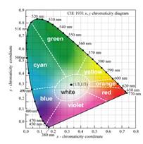
It is well known that white light can be synthesized from the three primary colors: red (Red), green (Green), and blue (Blue). The diagram shows the 1931 chromaticity diagram, where the dashed area in the center of the triangle represents the white light area. Gallium nitride LEDs generally emit light of only one color. White light lighting must also be achieved through the synthesis of RGB primary colors. The RGB primary colors can be directly emitted by LEDs or by using LEDs to excite fluorescent materials, obtaining primary or quasi-primary colors through secondary light conversion.
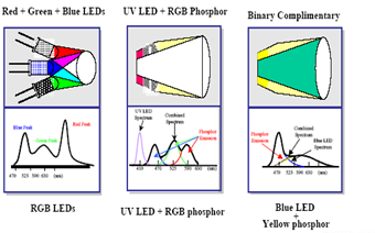
Therefore, there are two technical approaches to achieve gallium nitride LED white light lighting: one is using gallium nitride light-emitting diodes (LEDs) to excite fluorescent materials to convert into white light, referred to as “secondary light conversion white light technology”; the other is using LEDs to directly emit white light, referred to as “direct emission white light technology.”
➤3. Development Directions of LED White Light Lighting Technology
(1) Research and develop near-ultraviolet and deep ultraviolet LED devices to achieve high color rendering index “solid-state white light fluorescent lamps.” This white light technology has high color rendering index (CRI>90), high conversion efficiency (external quantum efficiency 43%), and high color reproduction, making it an ideal white light source.
(2) Research and develop III-nitride LEDs for direct emission white light technology.
(3) Research to improve LED luminous efficiency and light output, developing power-type LED devices.
Traditional incandescent lamps have a luminous efficiency of 16 lm/W, while fluorescent lamps have a luminous efficiency of 85 lm/W. Therefore, III-nitride LED white light lighting sources must achieve luminous efficiency of at least 100 lm/W to replace incandescent and fluorescent lamps, while also reducing costs.
8Optical Disc Storage and Laser Ranging, Laser Printing, Laser Instruments
Optical disc storage and laser ranging, laser printing, and laser instruments are another significant application area for semiconductor lasers. The wavelengths of lasers used in CD (compact disc) and DVD (digital versatile disc) are 780 nm and 670 nm, 650 nm, respectively, with lasers writing information onto discs or reading sound or light signals from them. The shorter the wavelength of the laser, the higher the storage density of the optical disc. The InGaN laser with a wavelength of 410 nm can significantly increase the storage capacity of optical discs. The InGaAlP lasers with wavelengths of 670-630 nm have replaced He-Ne lasers in many applications, finding important uses in laser ranging, laser printing, and laser medical instruments.
9Military Applications of Semiconductor Lasers
The AlGaAs high-power laser with a wavelength of 808 nm serves as the pump light source for high-power YAG (Yttrium Aluminum Garnet) solid-state lasers, replacing the original xenon gas lasers, eliminating the need for bulky power supplies and cooling systems, making solid-state lasers more efficient, compact, high-performance, and cost-effective, suitable for military applications such as laser radar and nuclear explosion simulation, nuclear fusion research. The underwater light transmission window is 590 nm, and the advent of blue-green lasers has opened doors for underwater communication. The most critical device in fiber optic gyroscopes for controlling direction during rocket and aircraft flight is the semiconductor super-radiant light-emitting diode.
10Environmental Protection
In nature, gases such as water vapor, methane, ammonia, carbon dioxide, carbon monoxide, hydrochloric acid, bromic acid, and hydrogen sulfide have sensitive absorption peaks in the 1.5-2.0 mm range. The wavelength of InAsSb or GaInAsSb variable quantum well lasers can reach the range of 1.0-4.0 mm, and the recently emerging quantum cascade lasers can reach wavelengths of 4.0-17.0 mm. These various lasers covering the infrared to far-infrared range serve as environmental guardians for atmospheric monitoring and detection.
The Future Development of Semiconductor Technology
1 The Revolution of Information Technology
Information transmission. The explosive increase in information volume demands ever-greater capacity for information channels. Not only text is transmitted online, but also music, images, television signals, etc.; not only wired, but also wireless; not only intercontinental, international, and intercity but also local area networks. Therefore, there is a need to develop new communication systems, such as Integrated Services Digital Network (ISDN) and multimedia technologies.
Information processing, including text processing, knowledge processing, image processing, as well as language recognition, image recognition, and intelligent processing. Artificial intelligence has achieved certain human-like intelligence through computers. For example: understanding and producing language, recognizing images, mathematical proofs, playing chess, composing music, and professional identification, medical diagnosis, etc. Computers will liberate people from some daily mental labor and, through the application of “thinking tools,” expand human wisdom to previously unimaginable levels.
2 Higher Integration
The mainstream processes of integrated circuits will undergo four stages of development: 65 nm (integrated circuit line width) in 2007, 45 nm in 2010, 33 nm in 2013, and 22 nm industrial production in 2016. For this, a series of key technologies and specialized equipment must be resolved, such as the research and development of new devices (non-traditional CMOS devices, new types of memory, logic devices, etc.), IC design, packaging, and testing technologies, as well as new photolithography machines, etching machines, and supporting equipment.
The size of semiconductor devices cannot be reduced indefinitely. If the device size shrinks to the de Broglie wavelength of electrons (10 nm), quantum effects will become more pronounced, necessitating the design of new semiconductor devices based on quantum mechanics principles.
3Development of Semiconductor Optoelectronic Devices Towards Longer and Shorter Wavelengths, Greater Power, and Higher Operating Frequencies
High-power laser arrays and quasi-continuous (QCW) devices, in addition to serving as pump sources for solid-state lasers, can also be directly used for material processing, medical applications, instrumentation, sensitive technologies, and printing, entering markets traditionally dominated by non-semiconductor lasers and replacing gas and solid lasers. AlGaN/GaN heterojunction bipolar transistors have good linearity, large current capacity, and uniform threshold current, primarily applied in high-power microwave systems that require high linearity and harsh working environments, such as military radar and communications; they can also be used in systems like intelligent robots that operate in harsh environments.
4 Integrated Optics and Integrated Optoelectronics
Systems composed of lasers, modulators, waveguides, gratings, prisms, and other passive optical components integrated on semiconductor films are called integrated optical systems. Integrated optical systems replace electrical interconnections with optical interconnections, offering advantages such as high bandwidth, large information capacity, low loss, fast speed, parallel processing, and resistance to electromagnetic interference in computer and communication systems. Silicon materials are low-cost and have mature processes, widely used in microelectronic devices. However, because they are indirect bandgap materials, they cannot be used as light-emitting devices. Currently, scientists are addressing the issue of light sources to achieve optoelectronic integration on silicon materials.
5Semiconductor Superlattice, Quantum Wire, and Quantum Dot Devices
Semiconductor superlattices, quantum wires, and quantum dots are low-dimensional structures that possess unique physical properties, such as quantum confinement effects and two-dimensional or one-dimensional characteristics of electron movement, enabling the fabrication of high-performance devices such as lasers, high electron mobility devices, optical bistable devices, and resonant tunneling devices. When the size and dimensions of the device are further reduced, making the average free path of electron movement greater than the device size, electrons will move coherently as a wave without scattering from impurities or lattice vibrations. Utilizing these characteristics, it is expected to manufacture ultra-fast, ultra-low power electronic devices. For example, quantum dot single-electron transistors will significantly reduce the power consumption of dynamic random access memory (DRAM).
6 Semiconductor Quantum Information Devices
Current processes have enabled the generation and detection of single photons on semiconductor quantum dots, making semiconductor quantum dots the most promising solid devices for quantum information processing (quantum computing, quantum communication). The rapid development of quantum information science and technology provides revolutionary theoretical and experimental methods for precision measurement, quantum computation, and secure communication. The key to quantum information is the use of the coherence of photons. Photons, as the most fundamental quantized entities in quantum theory, can easily realize the entire process of collecting, transmitting, copying, storing, and processing information, possessing unique inherent advantages as carriers of quantum communication and quantum computation. Therefore, photon-based quantum information processing devices are the foundation of various quantum information engineering, and their fundamental principle research and preparation will bring leapfrog advancements in computational science and communication capabilities.
7 Spintronic Devices
Currently, microelectronic devices use charge carriers to carry information. If a material can simultaneously utilize both the charge and spin properties of carriers as information carriers, it can manufacture devices with non-volatile, low power, high speed, and high integration advantages, potentially causing significant changes in electronic information science. Dilute magnetic semiconductors with magnetic ion doping and spintronics have emerged to meet this requirement. Experiments have shown that the spin coherence time in semiconductors has reached the nanosecond level, far exceeding the coherence time of charges, indicating promising applications for spintronics in future quantum computing and quantum communication. The main difficulty in realizing spin-based quantum computers is the precise control and maintenance of spin coherence; thus, many physical problems need to be studied and solved regarding how to generate spin-coherent electronic states and reduce spin decoherence.