
Source: WeChat Official Account “Chip Theory”
Introduction: Integrated circuits (chips) are manufactured layer by layer using photolithography technology. Therefore, the concept of “layers” exists in chip technology. So, how many concepts of “layers” are there in chip technology? Media reports say that Micron has launched a 176-layer 3D NAND flash memory chip; what does “layer” mean here? This article aims to provide a comprehensive analysis of the “layers” from a popular science perspective.
To explain the concept of “layers” in chip technology, one must first understand the design and manufacturing process of chips. This popular science content has been introduced in my other article “How Photolithography Has Become the Bottleneck Technology in Chip Manufacturing?”[5] This article describes how the photolithography process creates different semiconductor materials layer by layer on a silicon wafer according to the chip layout, ultimately forming a structured circuit component layer. This article will not elaborate further but will refer to the following two images from that article for clarification.
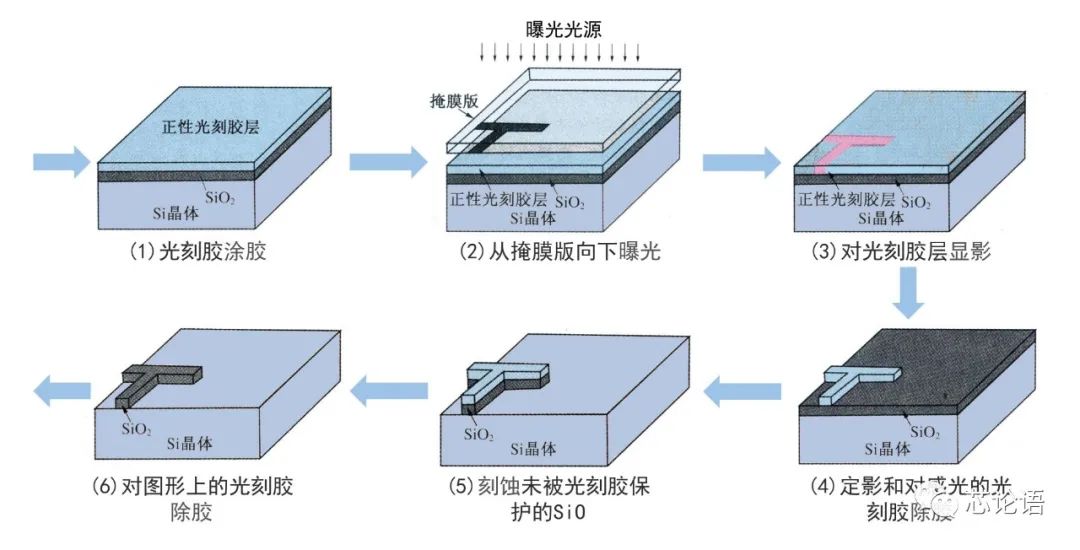
Figure 1. Schematic of the Photolithography Process
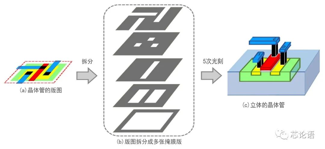
Figure 2. Stacking of Multiple Photolithography Steps to Form a 3D Circuit Structure
Figure 1 is a schematic of the photolithography process. Figure 2a shows the design layout of a transistor on the chip layout, which is separated into multiple mask patterns during the manufacturing preparation process and made into a set of multiple masks (Figure 2b). The chip manufacturing plant arranges the process in sequence, layer by layer, to create the patterns from the masks on the silicon wafer, forming a three-dimensional transistor (Figure 2c).
A chip can contain hundreds of millions to billions of transistors, interconnected to achieve the overall circuit function of the chip. After the various processes of the manufacturing technology, these transistors will be processed simultaneously. Moreover, a large number of identical chips are neatly arranged on the silicon wafer, and after the various processes of manufacturing technology, these chips will also be processed simultaneously.
1. Material Dielectric Layer vs Circuit Layer
Refer to Figure 3, where each layer pattern on the chip layout is marked in different colors. For each layer’s pattern, the manufacturing process will create a layer of shapes made of semiconductor materials or dielectrics on the silicon wafer. This article refers to these shape layers asMaterial Dielectric Layers. For example, P-type substrate layer, N-type diffusion region layer, oxide insulation layer, polysilicon layer, metal interconnect layer, etc. The number of layers in the chip layout basically corresponds to the number of material dielectric layers on the finished silicon wafer. Depending on the process arrangement, the number of material dielectric layers may also increase.

Figure 3. Correspondence between Transistors on Chip Layout and Three-Dimensional Transistors Manufactured on Silicon Wafer
Chip manufacturing is the process of creatingMaterial Dielectric Layers layer by layer on the silicon wafer according to the chip layout. The material dielectric layers stack together on the silicon wafer, forming all the circuit components on the entire chip and even on the entire silicon wafer. These mainly include transistors, memory units, diodes, resistors, interconnects, pins, etc.

Figure 4. Microscopic Schematic of Chips (From the perspective of Material Dielectric Layers, it appears as intersecting lines; from the perspective of Circuit Layers, it appears as a layer of circuit components laid out on the silicon wafer)
These circuit components appear structured and three-dimensional from the perspective of material dielectric layers. However, the circuit components are distributed in a plane on the silicon wafer and even on the entire silicon wafer; they are distributed in two dimensions (2D) and represent a planar layer. This article refers to the circuit components on the silicon wafer asCircuit Layers. The bare chip of such a chip package is the early traditional planar chip (2D chip).
2. Planar Structure Devices vs Lateral Structure Devices
In the circuit layer, the structure of early circuit components was arranged in a planar manner, referred to asPlanar Structure Devices. To increase the integration of chips, the size of circuit components, especially transistors, has been continuously reduced according to Moore’s Law. When the device size can no longer be reduced, the industry invented a vertical structure for circuit components to reduce the chip area. Some refer to this vertical device as a three-dimensional (3D) or volumetric structure device. However, I believe it is more accurate to call itLateral Structure Devices. Because whether planar structure devices or lateral structure devices, although they appear three-dimensional from the perspective of material dielectric layers, they are all distributed in a plane on the silicon wafer, representing only one layer of circuit components without any volumetric concept.

Figure 5. Planar and Lateral Transistor Structures
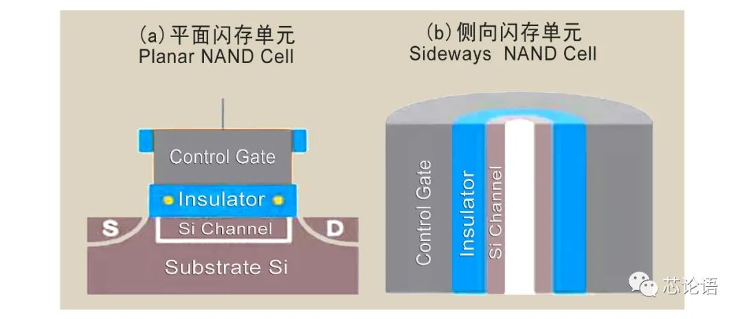
Figure 6. Planar and Lateral Flash Memory Cell Structures
Early chip manufacturing processes were quite traditional, allowing only one circuit layer to be manufactured on the silicon wafer. Taking the transistor shown in Figure 5 and the flash memory cell shown in Figure 6 as examples, the structure of circuit components, whether planar (Figure 5a, Figure 6a) or lateral (Figure 5b, Figure 6b), does not have stacking of components above them. After the manufacturing, dicing, packaging, and testing of the circuit layer, the entire chip manufacturing process is completed. This type of single circuit layer chip is the early traditional planar chip (2D chip).
3. Multi-layer Chip Stacking Packaging, Forming Pseudo-3D Chips
With advancements in chip packaging technology, the industry has invented multi-layer chip stacking packaging technology to reduce chip size. Initially, stacking packaging involved stacking multiple bare chips together, connecting signals between the chips through bonding technology to form a complete internal system, and then routing external signals through package pins, ultimately packaging them into a complete chip (Figure 7a). Later, the industry invented Through-Silicon Via (TSV) technology, where signals between stacked bare chips are connected through TSV, forming a more compact multi-chip stacked packaging chip (Figure 7b).
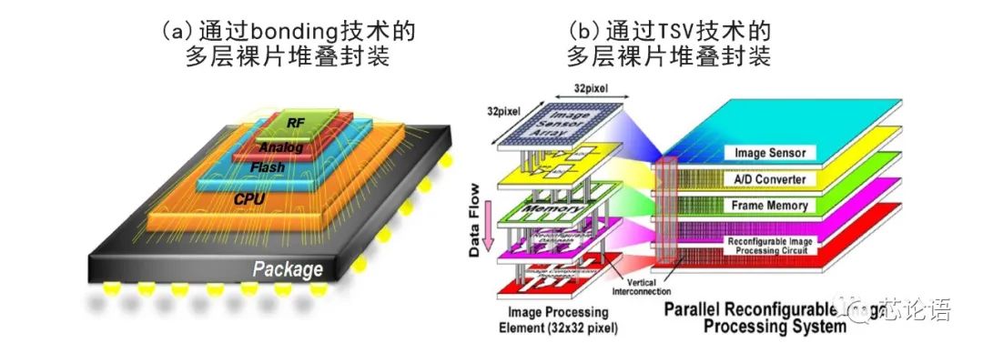
Figure 7. Schematic of Multi-chip Stacked Packaging (Source: Jin-Fu Li, EE, NCU)
This type of chip contains multiple circuit layers internally, which can be referred to as volumetric chips or 3D chips. However, this 3D chip is formed during the packaging phase through multi-layer bare chip stacking; from the perspective of chip manufacturing, this 3D chip can only be considered a pseudo-3D chip.
4. Multi-layer Circuit Layer Stacking Manufacturing, Forming True 3D Chips
Currently, chip manufacturing technology has developed to an advanced level. To save silicon area, after completing the manufacturing of the lower circuit layer, another circuit layer can be made on top of it, forming two or even multiple circuit layers stacked on the silicon wafer during the chip manufacturing phase, achieving the production of true 3D chips. This results in what is truly a volumetric chip, also known as a 3D chip.
This technology is currently mainly used in the manufacturing of highly regular chips such as 3D NAND flash memory. Memory cells adopt lateral structures. Generally, if a flash memory chip claims to be N-layer NAND flash, it must have at least NCircuit Layers. Currently, Samsung’s 3D V-NAND memory cell layers have gradually increased from 2 layers in 2009 to 24 layers, 64 layers, and then to 96 layers in 2018[2], with the development of 128-layer V-NAND flash completed and mass production achieved in August 2019. Samsung plans to mass-produce the 7th generation V-NAND flash in the second half of 2021, increasing the stacking layers to 176 layers. Micron has released the fifth-generation 176-layer 3D NAND flash memory chip using the latest technology[4].
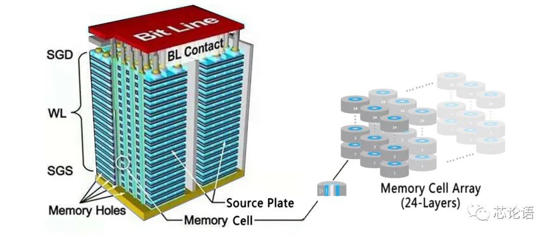
Figure 8. Schematic of Multi-Circuit Layer Stacking Structure of 3D NAND Flash Memory Chip
(Source: Reference 2, compiled by the author)
In China, Yangtze Memory Technologies successfully developed the first 3D NAND flash memory chip in July 2017; in the third quarter of 2018, 32-layer products achieved mass production; and in the third quarter of 2019, 64-layer products achieved mass production. They have now announced the successful development of a series of 128-layer 3D NAND flash memory chips[3]. The rapid development of Yangtze Memory Technologies’ 3D NAND flash technology benefits from its unique XtackingTM technology, which separates the manufacturing of the storage array (Cell Array) and peripheral control circuitry (Periphery) before merging them into a package.
Figure 9. Demonstration of Yangtze Memory Technologies’ XtackingTM Technology (Source: Yangtze Memory Technologies official website)
According to reports, Micron’s latest generation of 176-layer 3D NAND will directly replace the 96-layer version. It is known that Micron’s first batch of 176-layer 3D NAND adopts a design that merges two 88-layer chips (stacking 512Gbit TLC flash memory). This chip technology has switched to a charge trap storage cell scheme, which seems to have significantly reduced the thickness of each layer. Currently, the thickness of the 176-layer bare chip is only 45μm, the same as Micron’s 64-layer floating gate 3D NAND. The thickness of the 16-layer bare chip stacked packaging is less than 1.5 mm, suitable for most mobile/storage card usage scenarios[4].
Conclusion: This article clarifies the concepts of Material Dielectric Layers and Circuit Layers in chip technology through the introduction of photolithography and chip manufacturing technology, thereby providing a clearer understanding of what constitutes a 2D chip and what constitutes a 3D chip. It also highlights that current 3D flash memory chips can integrate up to 176 layers of circuit layers during manufacturing. Moreover, these 3D chips can also achieve up to 16 layers of bare chip stacking during packaging. In a flash memory card with a thickness of less than 1.5mm, there can be as many as 2816 layers of circuit layers in operation, showcasing the intricacies of chip technology.
References:
1. Helen, What is 3D NAND? What Advantages Does It Have Compared to 2D NAND?, China Flash Market:https://www.chinaflashmarket.com/Instructor/163856, 2018.11.6
2. Tianji Network, An Article to Help You Understand Samsung’s Fifth Generation V-NAND Technology, Sohu:https://www.sohu.com/a/299871029_115479, 2019.3.8
3. Love Micro, Yangtze Memory Technologies Announces Successful Development of 128-Layer 3D NAND Flash Chip Series, Electronic Enthusiasts:http://www.elecfans.com/d/1286790.html, 2020.9.2
4. cnBeta, Micron Releases Fifth Generation 3D NAND Flash Stacking Reaching 176 Layers, Baidu:https://baijiahao.baidu.com/s?id=1682951127434407581, 2020.11.10
5. Tian Gao Yun Dan, How Photolithography Has Become the Bottleneck Technology in Chip Manufacturing?, Tencent:https://mp.weixin.qq.com/s/wC4Q31J26DGnHZFaA6ldwQ, 2020.11.30
Editor: Lemon