Previously, we discussed the on-chip interconnect bus, but having just the bus is not enough; we also need on-chip bus protocol support. Only with the protocol can we operate the registers accurately.
When it comes to on-chip bus protocols, there are many, such as the AMBA bus used by ARM, the Wishbone bus by Silicore, and the Avalon bus by Altera. You can search for more information about these buses online.
The on-chip bus protocol seems advanced at first glance, but it is essentially an agreement on how two parties communicate. With this communication method, both parties can communicate accurately and quickly.
Below, I’ll illustrate using the AMBA bus from ARM as an example, as I have researched this bus. However, once you understand one type of on-chip bus, learning about others becomes much easier.
Currently, AMBA mainly has three types of bus protocols:
1. AHB
2. APB
3. AXI
The on-chip interconnect bus protocol used by Xilinx’s Zynq chip is AXI4, which is a more advanced bus protocol.
Next, I’ll explain the APB bus, as it is the simplest among the three protocols.
Previously, a question was raised: the CPU can only operate on registers within one clock cycle, but what if certain register operations require several clock cycles? In that case, the pipeline needs to pause until the register operation is completed before resuming to execute subsequent instructions. The CPU needs the APB protocol to know when to pause and when to resume the pipeline.
First, let’s take a look at the APB protocol interface:
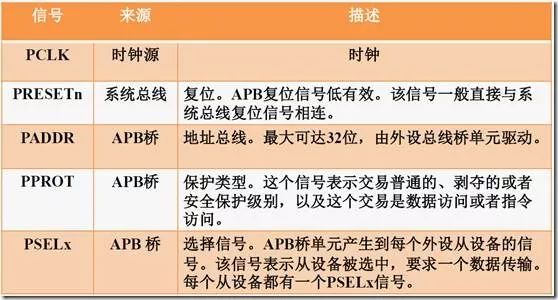
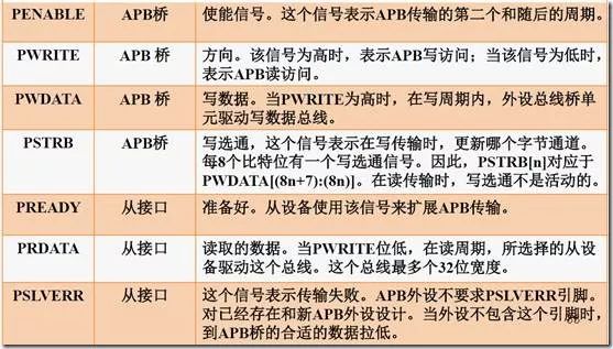
Just looking at these interface signals might not give you much insight, but examining the timing diagram helps us understand the APB protocol better.
Since register operations involve both read and write processes, the APB protocol is divided into read transfers and write transfers.
For read transfers:
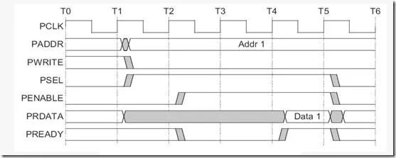
What can we infer from the timing diagram?
For reads, the PWDATA signal is not used. PADDR is the address, which, as mentioned earlier, is the address of the register. The second signal, PWRITE, indicates whether it is a read or write operation; since this is a read, it is 0. The third signal, PSEL, is the chip select signal, which is the register enable signal mentioned in the previous blog about bus interconnects. The PENABLE signal indicates the start of the transfer.
Since reading data may require multiple clock cycles, there is a signal called PREADY, which indicates whether the data read is valid. When it is high, the CPU can read the register data.
Thus, for the CPU, when it needs to read data from an external register, it first pauses the pipeline, generates the PADDR, PWRITE, PSEL, and PENABLE signals according to the APB protocol for the read transfer, and then waits for the PREADY signal. Once it is high, indicating that the data read was successful, the CPU reads the data from PRDATA, completes the read transfer, and then resumes the pipeline.
For write transfers:
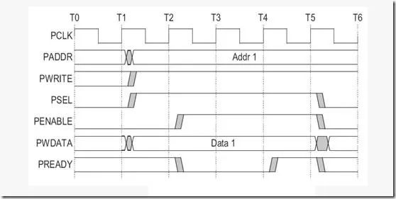
Once you understand the read transfer, the write transfer is also straightforward.
Since this is a write operation, the PRDATA signal is not of concern. The other signals are the same as those for the read transfer, with the addition of the PWDATA signal, which carries the data to be written to the register. Similarly, writing may also take multiple clock cycles, so the PREADY signal is used to indicate whether the data can be successfully written. When it is 1, it indicates that the data can be successfully written, and the CPU does not need to wait any longer.
Therefore, for the CPU, when it needs to write data to an external register, it first pauses the pipeline, generates the PADDR, PWRITE, PSEL, PENABLE, and PWDATA signals according to the APB protocol for the write transfer, and then waits for the PREADY signal. Once it is high, it indicates a successful write, completing the write transfer, and then resumes the pipeline.
Of course, the APB protocol has other interfaces, but these are used to extend certain functionalities, and you may choose not to use them.
With the protocol mechanism described above, the CPU’s operations on external registers can be carried out accurately. Once the bus protocol is introduced, the CPU is no longer simply sending address and data buses; at this point, the control bus comes into play. The control bus is a collection of necessary signals specified in the interconnect bus protocol being used.
For the APB protocol, because it is relatively simple, the control bus protocol is also simple, consisting of just the PADDR, PWRITE, PSEL, PENABLE, and PREADY signals. However, if other protocols are used, the control bus can become complex; for example, the AXI4 protocol has 5 channels and dozens of interfaces, making it much more complicated than APB.