▲ Click the above 21Dianyuan to follow us
This article is a original entry for the “Eighth Original DIY Power Supply Technology Experience Sharing Competition” held by the 21Dianyuan Community. Thanks to the author Feihong Tanyue for their hard work.
In the previous issue, we shared the “Characteristics of Power Devices in Modular Power Supplies”. Today, we will discuss the common power topologies used in modular power supplies.
🔗 Link
Understanding Modular Power Supplies (Part 1)
Characteristics and Simulation Analysis of Common Topologies in Modular Power Supplies
What we commonly refer to as switch-mode power supplies generally refers to hard-switching power supplies, which typically have significant switching losses. The higher the frequency, the more severe the switching losses.
The fundamental reason for the compact size of modular power supplies is their significant increase in operational frequency. Using conventional power topologies under these conditions can be counterproductive.
So, is there a type of power topology that can effectively address switching losses? Certainly, this is the soft-switching power topology.
The switching of power MOSFETs does not occur instantaneously; during the transition from off to on or from on to off, both voltage and current are present simultaneously.
In other words, we only need to control the Vds voltage or Ids current during the switching process of the power MOSFET, making it zero before the power MOSFET is fully turned on or off, thus solving the switching loss issue.
With this idea in mind, the meaning of soft-switching power topology becomes clear.
What is Soft-Switching Power Supply?
In simple terms, during the on and off processes of soft-switching power supply devices, either the voltage applied to them is zero (zero-voltage switching) or the current flowing through the switching device is zero (zero-current switching).
This type of power topology effectively reduces high-frequency switching losses, facilitating the high-frequency and miniaturization of power modules, and improving efficiency.
Soft-switching power supplies can be roughly classified into eight categories::
▫ Full Resonant Converter
▫ Quasi-Resonant Converter
▫ Multi-Resonant Converter
▫ Zero-Voltage Switching Pulse Converter
▫ Zero-Current Switching Pulse Converter
▫ Phase-Shifted Full Bridge Zero-Voltage Converter
▫ Phase-Shifted Full Bridge Zero-Current Converter
▫ Active Clamp Converter
I have been working in the power supply field for about eight years, and the soft-switching power supply topologies commonly used in the industry are actually just a few, namely:
▫ QR Flyback Quasi-Resonant Power Topology
▫ Active Clamp Forward Power Topology
▫ LLC Half-Bridge Topology
▫ Phase-Shifted Full Bridge Topology
Control Methods for Resonant Converters
The control method for resonant converters is generally PFM control, which is directly linked to the frequency characteristics and output load changes. As the load increases, the frequency rises; as the load decreases, the frequency falls.
According to the process of energy conversion involving resonant components, they can be classified into quasi-resonant converters, multi-resonant converters, and full resonant converters.Essentially, this applies the principle of resonance to make the voltage or current of the power devices in the switch-mode power supply change in a sinusoidal or quasi-sinusoidal manner. When the voltage is zero, the device turns on; when the current is zero, the device turns off, thus making the losses of the power devices during on and off processes nearly zero, solving the switching loss issue.
Based on the connection methods of the resonant components, they can be divided into series resonant converters and parallel resonant converters. The active clamp absorption circuit can suppress the transient voltage or current of the switching device, reducing the voltage stress and current stress on the switching transistor, significantly reducing switching losses. At the same time, this type of topology can feedback the absorbed energy to the grid, reducing switching losses and improving the power conversion efficiency.
▫ The chip commonly used in quasi-resonant flyback converters is NCP1307
▫ The widely used series resonant LLC converter schemes are L6562+L6599 or NCP1393
▫ The commonly used control chip for phase-shifted full bridge converters is UC3875
▫ The commonly used chip for active clamp is MA3410
I have summarized the working principles of conventional soft-switching power supplies, and next, I will consider using simulation software to discuss the principles of the various types of soft-switching power supplies mentioned above.
Conventional flyback switch-mode power supply circuits are quite simple, but the switching of power MOSFETs has significant switching losses, and the transmission efficiency of flyback power supplies generally only reaches 70%-80%.
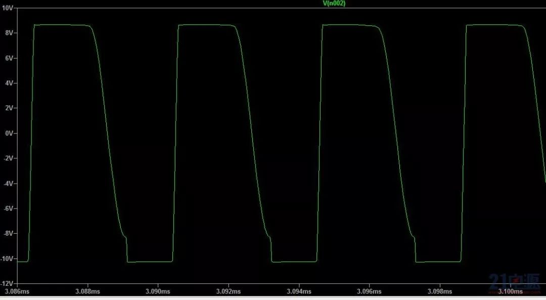
Quasi-resonant flyback power supplies detect the resonant waveform voltage of stray capacitance and the magnetizing inductance of the transformer. After several resonant cycles, when the voltage at the drain-source level is at its lowest point, the power MOSFET is turned on, minimizing the turn-on loss of the power MOSFET.
Quasi-resonant power supplies differ from conventional resonant power supplies in the resonant process. Conventional resonant power supplies have resonant components that actively participate in the entire energy change process (the oscillation waveform is sinusoidal); the quasi-resonant mode only participates in the resonant process during one phase of the entire energy conversion of the power supply, which is during the switching transition (the waveform is still close to a square wave), using resonance to complete the switching transition at zero voltage (or minimum voltage).
The power MOSFET in the quasi-resonant power supply turns on at the valley, thus reducing turn-on losses. The turn-on of the power MOSFET is driven by the control IC detecting the valley voltage.
I simulated the QR flyback power supply topology for everyone to analyze.
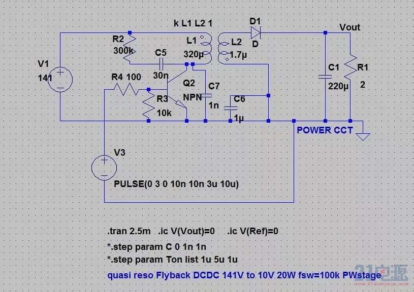
QR Power Topology
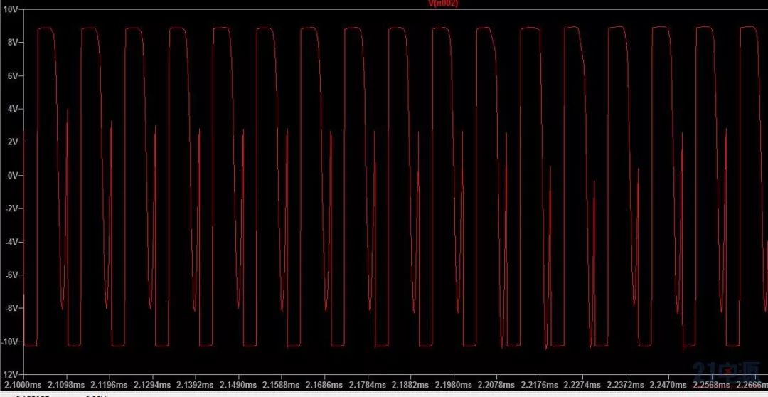
Gate Drive Waveform
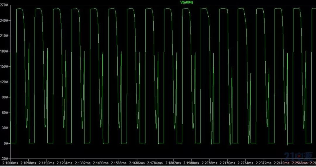
Drain Waveform
Output Waveform
The feedback control system of switch-mode power supplies is generally divided into three categories, simply speaking as first-order compensation network, second-order compensation network, and third-order compensation network.
This classification method is mainly based on the number of poles and zeros. A simpler and more intuitive classification method is PI, PD, and PID control methods, which are simply three types of compensation methods commonly used in the field of automatic control.
Since conventional power supply feedback loops do not have very high speed and accuracy, and are convenient for simulation modeling, I have generally used PI control loops in subsequent power supply simulations.
First, I will post the closed-loop simulation circuit of the QR flyback power supply for everyone to analyze, and I will also post the node waveforms later.
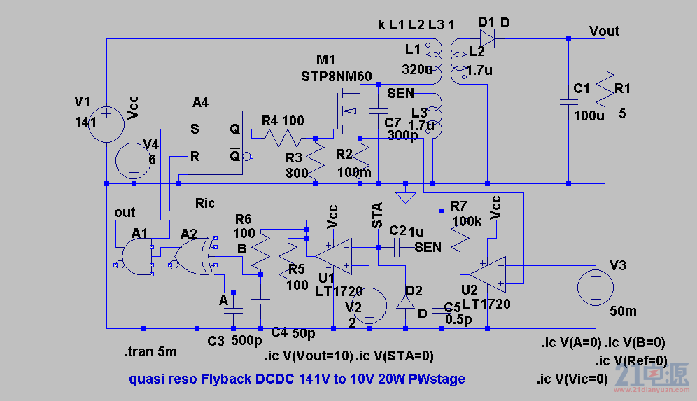
Closed-Loop QR Flyback
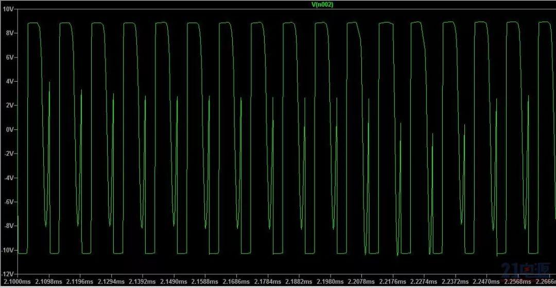
The following figure shows the gate, drain, and secondary waveforms of the closed-loop QR flyback power supply. The QR power supply is not fundamentally different from conventional flyback power supplies; the key technology is the valley detection drive of the control chip.
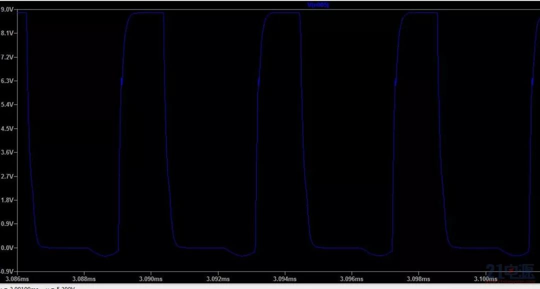
Closed-Loop Gate Drive Waveform
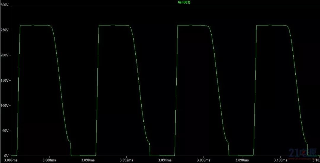
Closed-Loop Drain Waveform
Closed-Loop Secondary Waveform
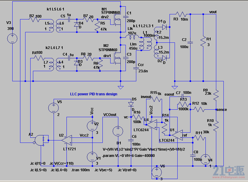
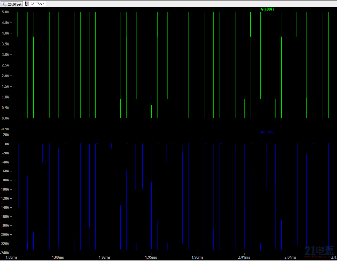
LLC open-loop power supply simulation and node waveforms. Analyzing the simulation circuit of this circuit should make understanding the principles of LLC easier.
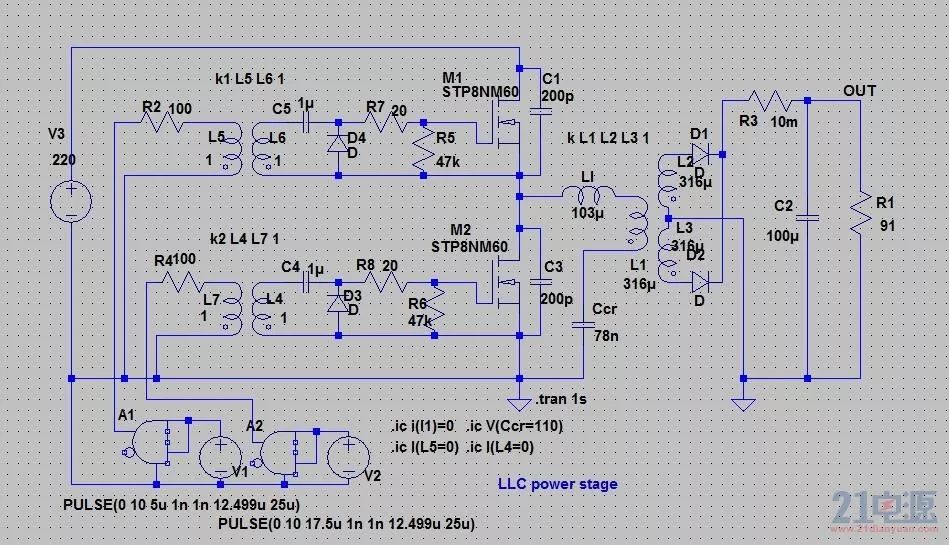
LLC Open-Loop Simulation Circuit
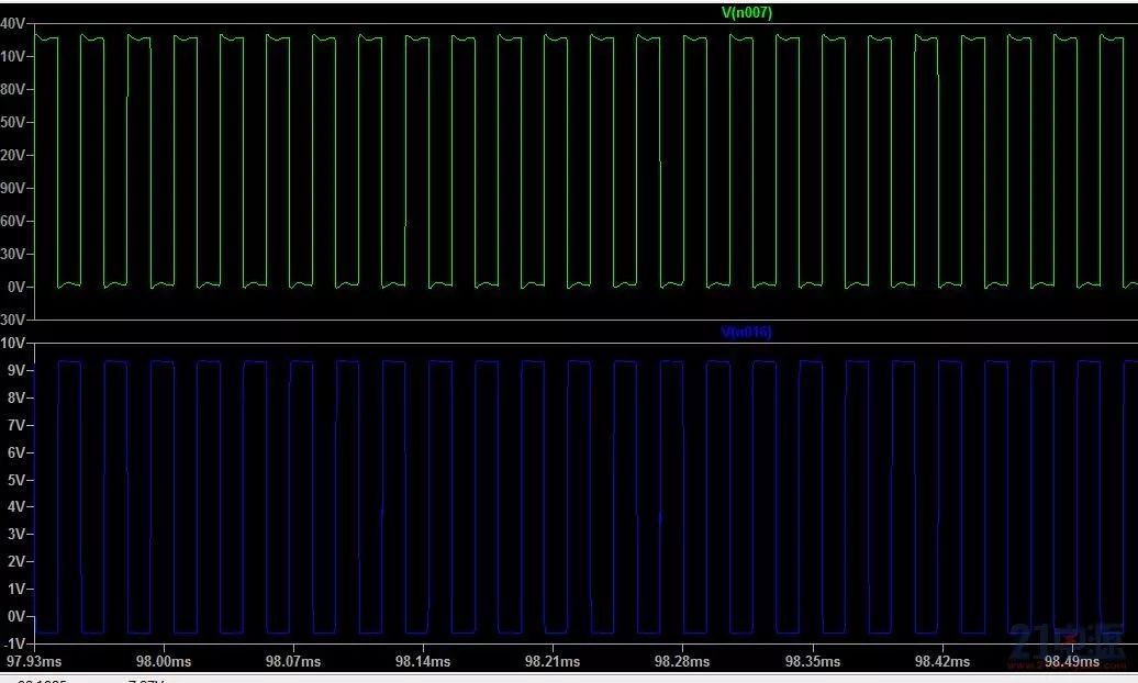
Primary Upper and Lower Tube Drive Waveform
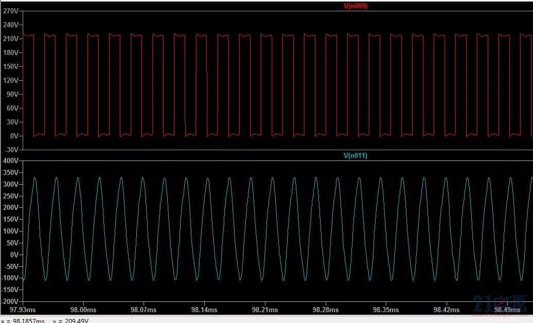
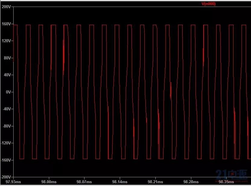
Primary Voltage Resonance Waveform
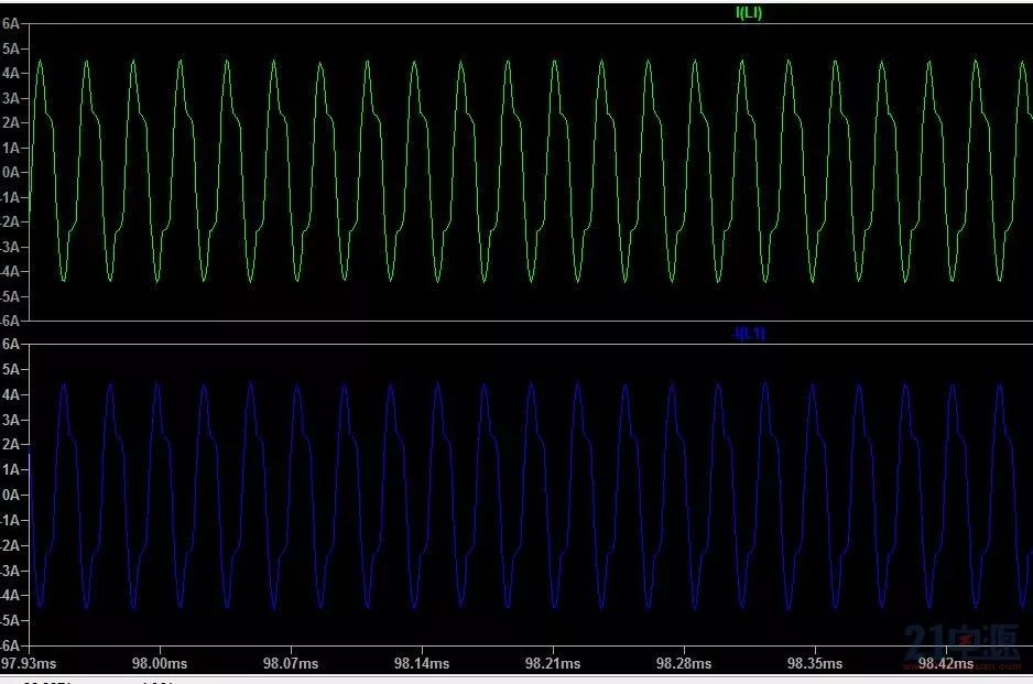
Primary Current Resonance Waveform
Secondary Voltage Drive Waveform
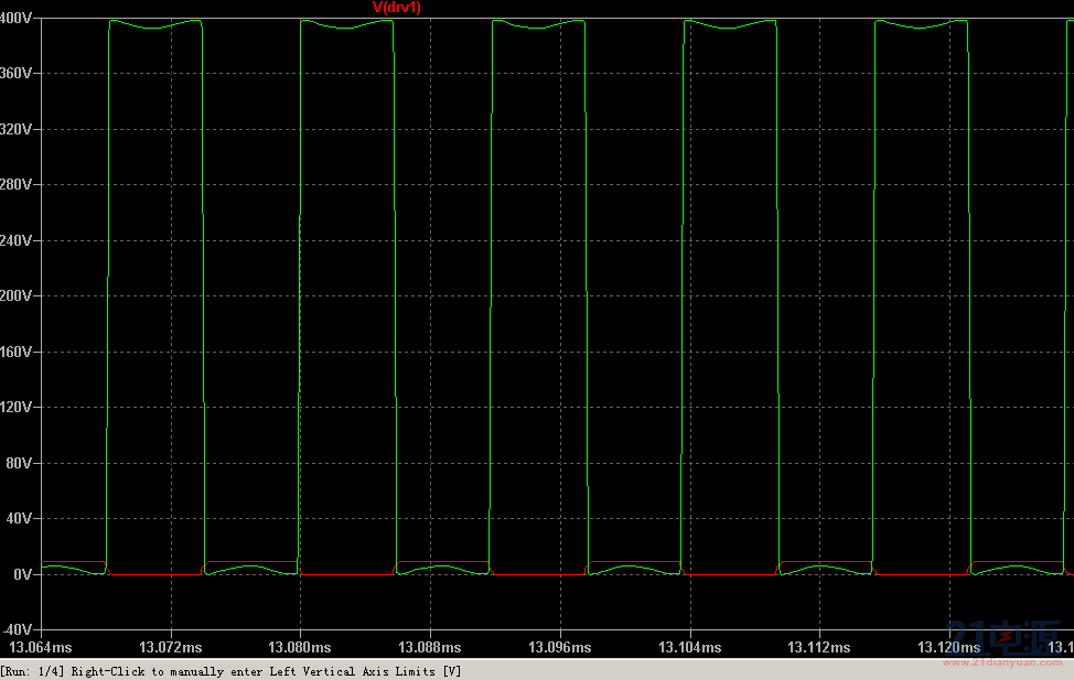
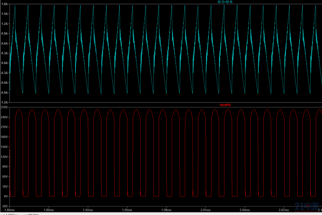
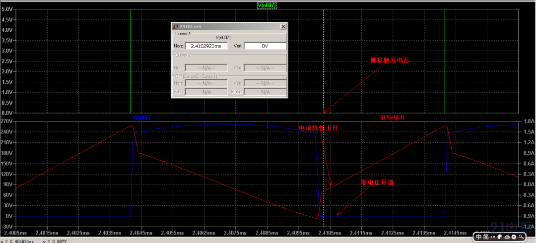
Closed-loop LLC control, half-bridge voltage and current waveforms. From this, it can be seen that this power topology achieves zero-voltage turn-on.
Closed-Loop LLC Topology
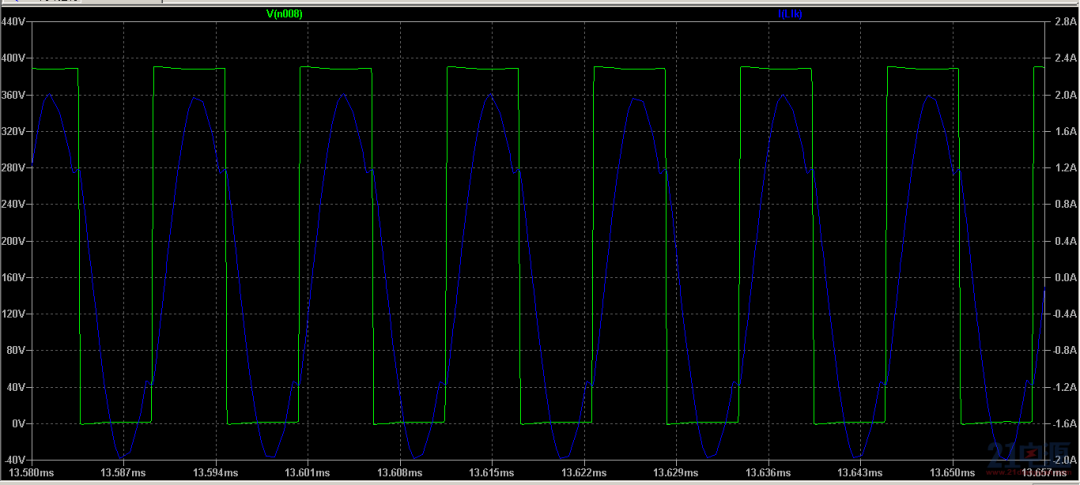
Primary Zero-Voltage Turn-On
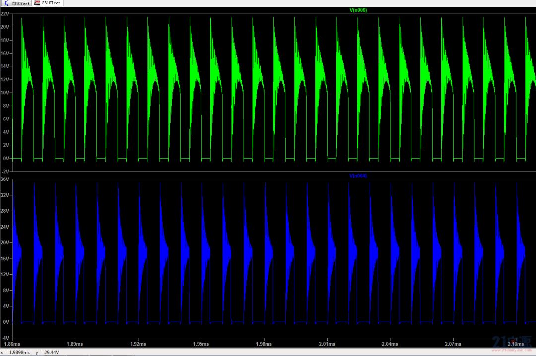
LLC topology secondary diode voltage and current waveforms. From the waveforms, it can be seen that the secondary of this power supply achieves zero-current turn-off.
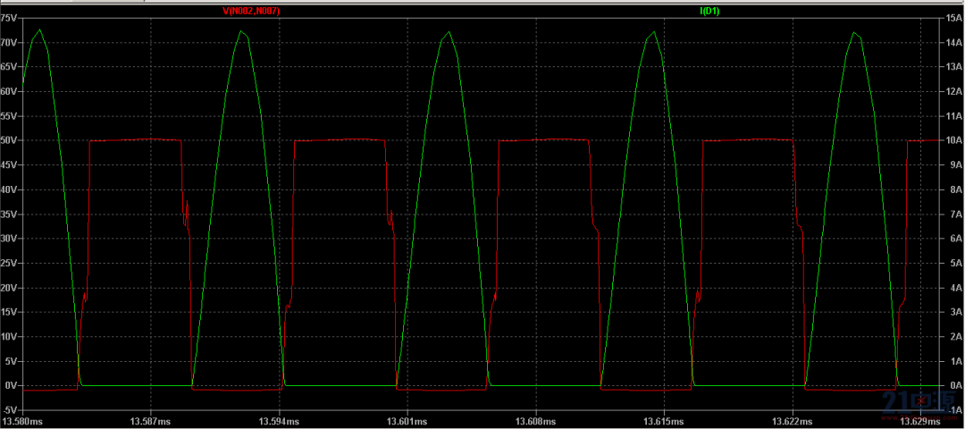
Secondary Zero-Current Turn-Off
Upper and lower tube drive waveforms and output voltage waveforms, with output resistance ranging from 1R to 10R, stepping by 2R.
Upper and Lower Tube Waveforms
Secondary Output Waveform
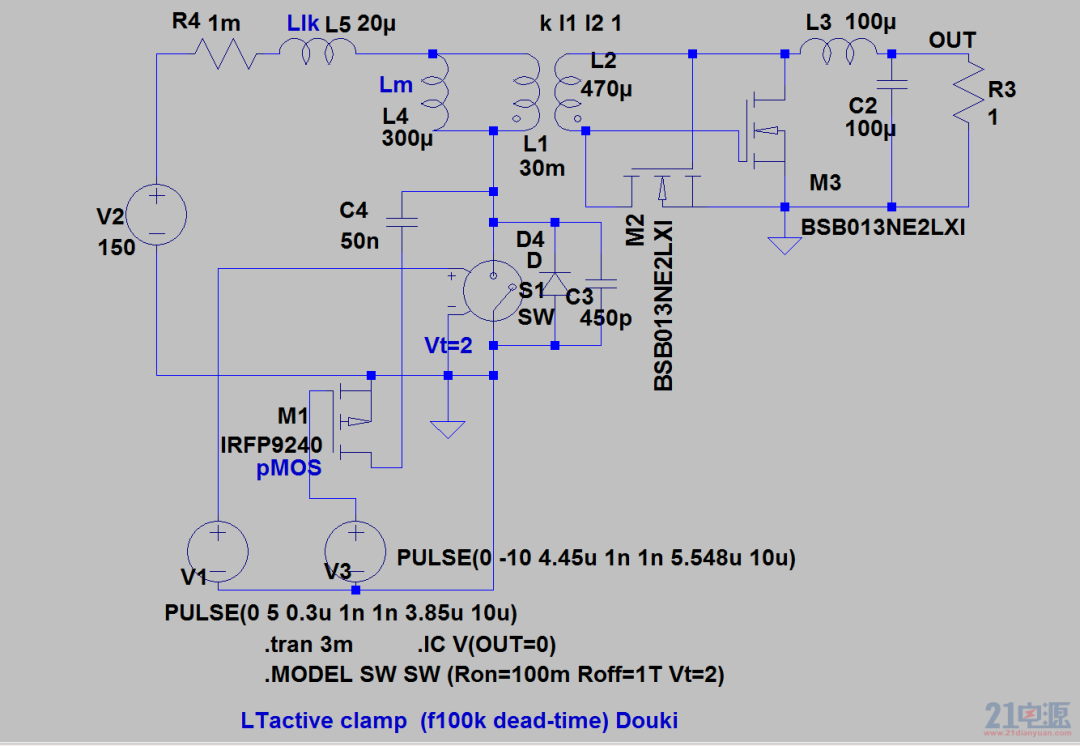
Simulated the open-loop circuit of the active clamp topology.
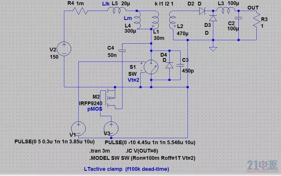
Active Clamp Forward Open-Loop
Next, here are the waveforms of each node of this topology.
Primary Upper and Lower Tube Drive Waveform
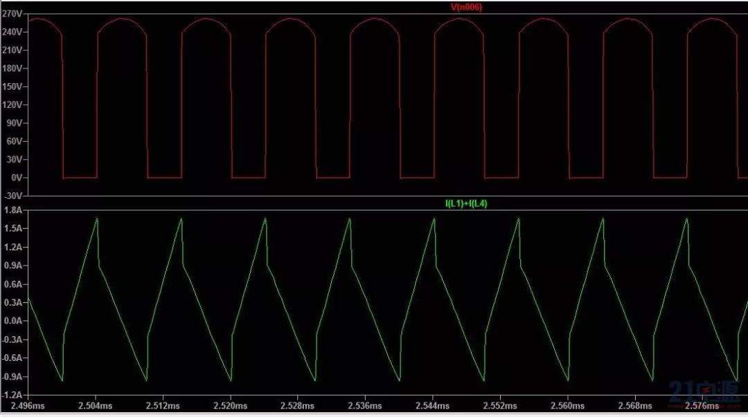
Primary Power Tube Voltage and Current Waveform
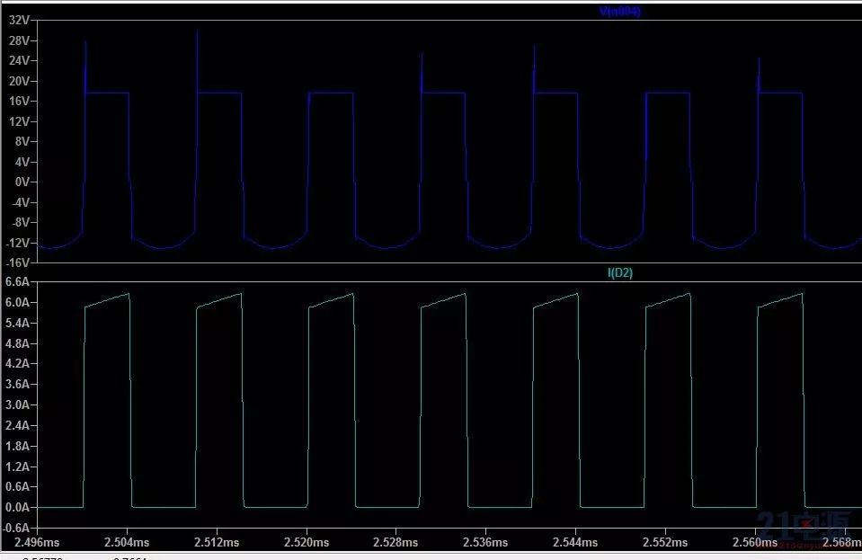
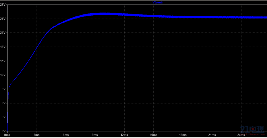
Secondary Voltage and Current Waveforms
Added synchronous rectification technology to the secondary of the active clamp forward topology. The simulation seems to perform well; let everyone take a look.
Synchronous Rectification Active Clamp Forward Topology
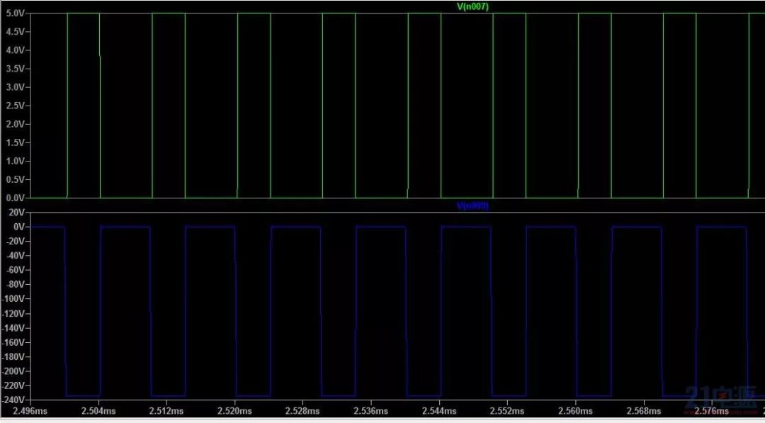
Primary Upper and Lower Tube Drive Waveform
Primary Main Power Tube Drain Voltage and Current Waveform
Secondary Upper and Lower Tube Drive Waveform
Active Clamp Forward Circuit
We know that forward, push-pull, half-bridge, and full-bridge all originate from Buck power supplies. However, compared to forward power supplies, the former can achieve self-magnetic reset functionality, as their transformers operate in the first and third quadrants; while the forward topology operates in the first quadrant and cannot achieve self-magnetic reset functionality, requiring additional magnetic reset circuits to assist the transformer in achieving magnetic reset functionality. Additionally, to ensure sufficient magnetic reset for the forward transformer, its duty cycle must be less than 0.5.
Is there a good way to improve this characteristic of the forward topology?
Of course, this is the active clamp forward topology. To put it simply, the active clamp can allow the duty cycle of the forward topology to exceed 50%, reducing the current stress on the switching transistor, while also achieving soft-switching (ZVS) for the main power tube, reducing switching losses and facilitating the high-frequency operation of the power supply. Additionally, the transformer core can also be magnetized bidirectionally, improving core utilization.
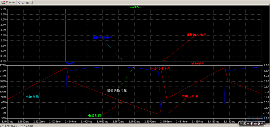
Taking the lower tube active clamp as an example: From the node waveforms, it can be seen that the voltage across the parasitic capacitance of the main power tube is zero, at which point the power MOSFET is triggered to turn on, and the transformer magnetizing current rises from negative to positive.
Main Power MOSFET Node Waveform
The waveforms of the turn-on and turn-off of the primary main power tube, as well as the detailed waveforms of the auxiliary power tube nodes are as follows.
Main Power Waveform
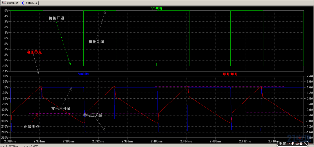
Detailed Waveform of Auxiliary Power Tube Nodes
ACF closed-loop control simulation schematic diagram and primary upper and lower tube node waveform parameters.
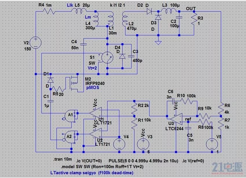
ACF Closed-Loop Control Circuit
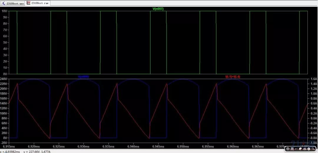
Primary Upper Tube Drive Waveform and Drain Voltage Current Waveforms
Primary Lower Tube Drive Waveform and Drain Voltage and Current Waveforms
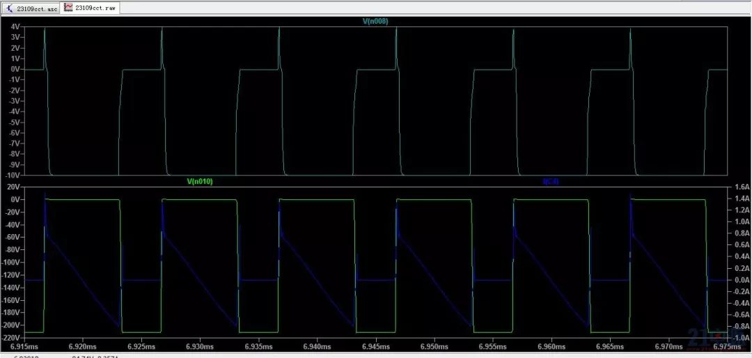
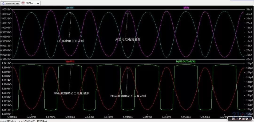
Compared the voltage and current waveforms sampled by the output terminal voltage divider of the closed-loop ACF topology before and after PID adjustment.
Comparison Waveform
From the comparison waveforms, it can be seen that for this ACF topology, PID control essentially represents voltage mode feedback control. After introducing PID control, the output characteristics of the power supply have changed significantly, with improvements in both dynamic response and steady-state characteristics.
Feedback Characteristics of Switch-Mode Power Supplies
1 First-Order Compensation Network
From the simulation circuit analysis of its output phase-frequency characteristics, it can be seen that the integrator only enhances the DC gain but does not provide any phase enhancement. At the same time, the first-order compensation integrator only provides one pole.
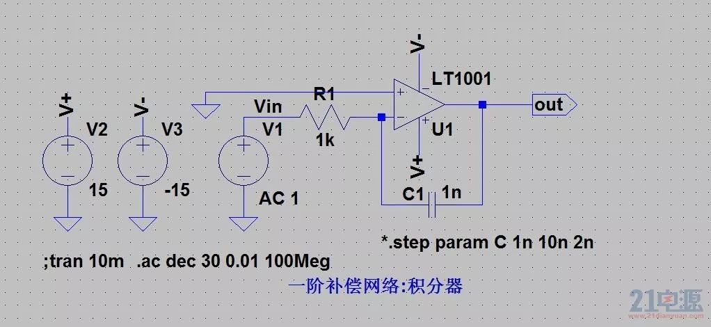
Integrator Circuit
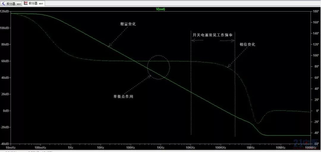
Integrator Compensation Network Output Phase-Frequency Characteristics
2 Second-Order Compensation Network
The simulation analysis of the second-order compensation network of switch-mode power supplies is shown in the figure, where the phase-frequency characteristics and transfer function characteristics of the second-order compensation network are indicated.
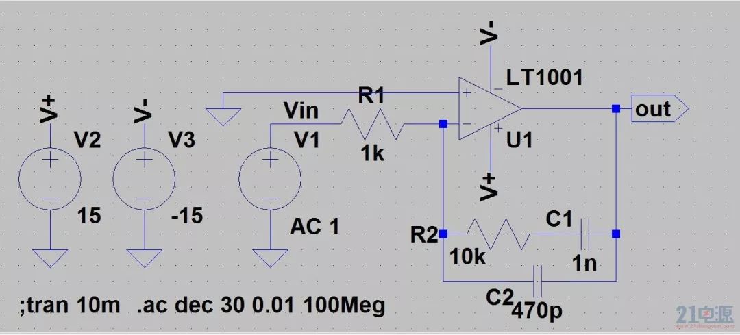
Second-Order Compensation Network Circuit
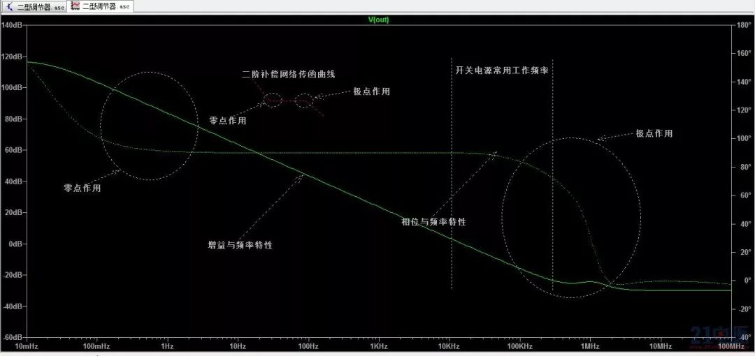
Second-Order Compensation Network Phase-Frequency Characteristics
3 Third-Order Compensation Network
The following figure shows the transfer function characteristics curve of the third-order compensation network.
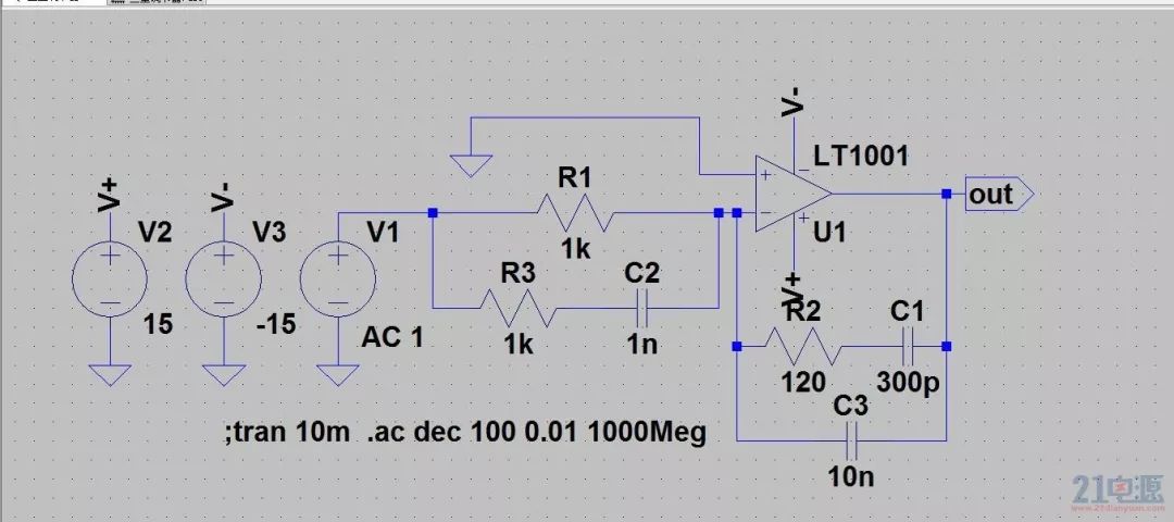
Third-Order Compensation Circuit
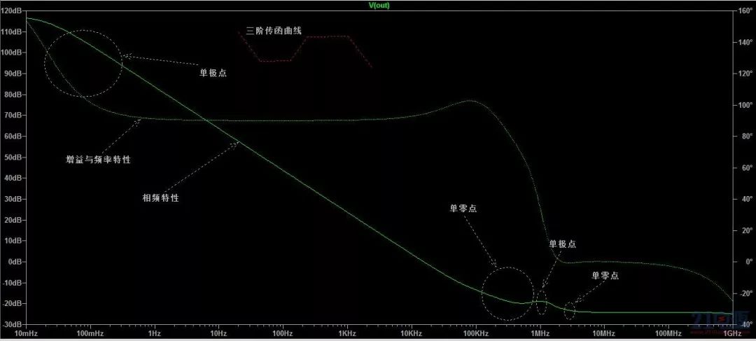
Third-Order Compensation Network Transfer Function Characteristics
Related amplitude-frequency characteristics and phase-frequency characteristics of PID control. First, let’s talk about the transfer function characteristics of the proportional amplifier.
Proportional Amplifier
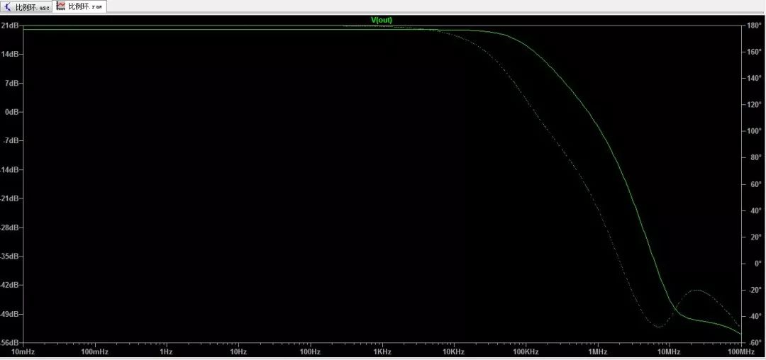
Proportional Amplifier Transfer Function Characteristics Curve
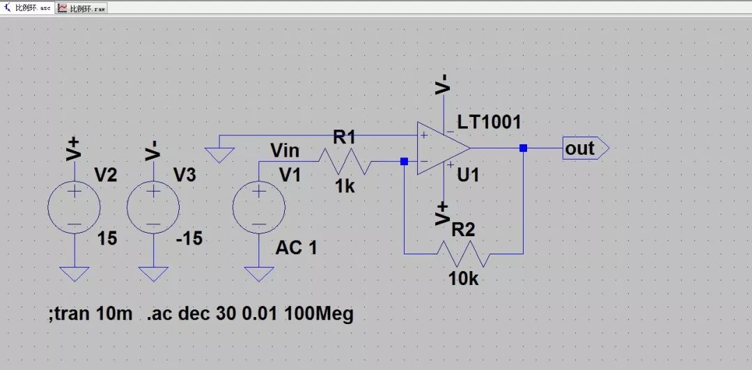
Next is the proportional-derivative amplifier, commonly known as the PD controller.
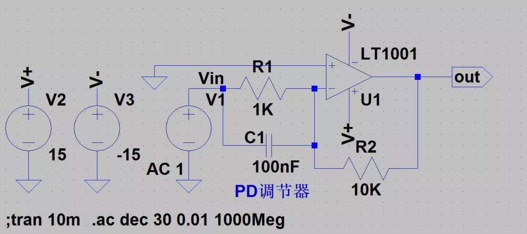
Proportional-Derivative Amplifier Circuit
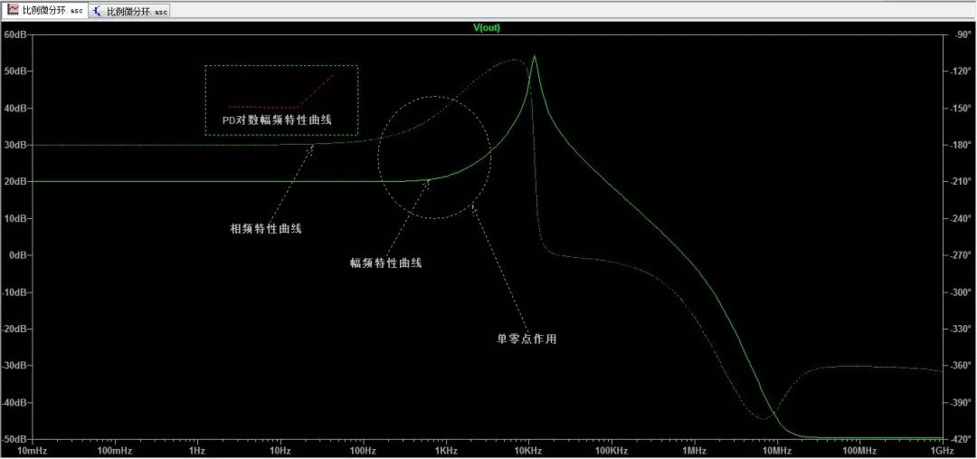
Proportional-Derivative Amplifier Transfer Function Characteristics Curve
The proportional-integral circuit schematic diagram and transfer function curve.
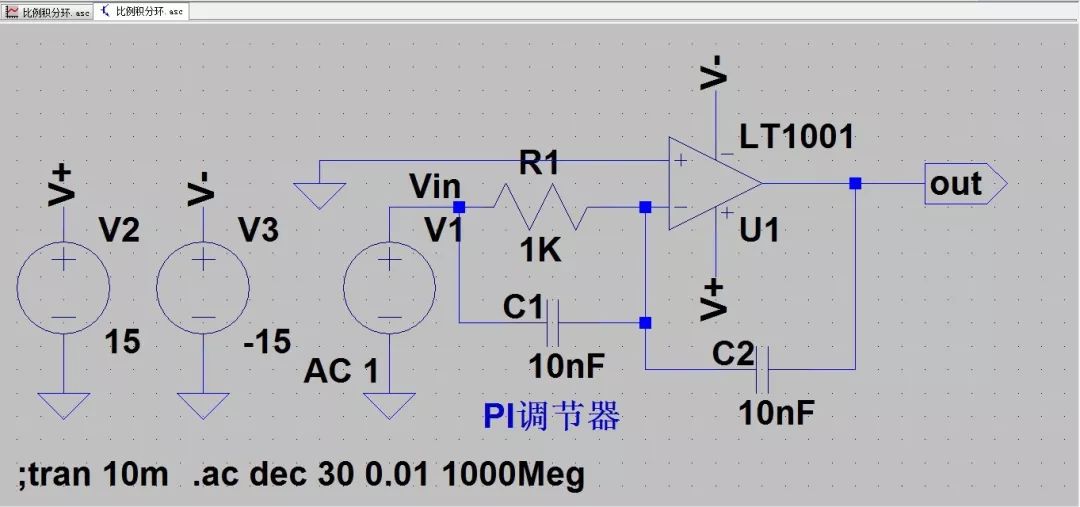
Proportional-Integral Circuit Schematic Diagram
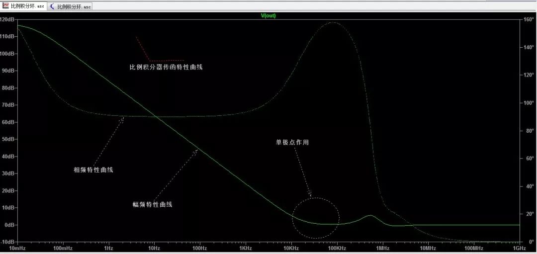
Proportional-Integral Transfer Function Curve
Transfer function curve characteristics of the proportional-integral-derivative circuit.
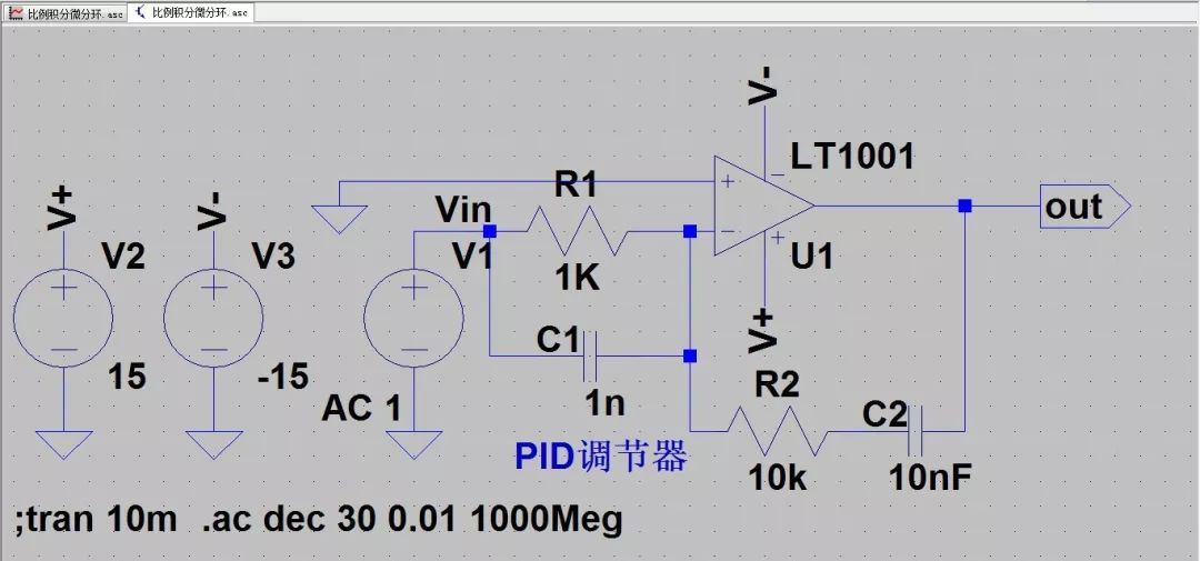
Circuit Diagram
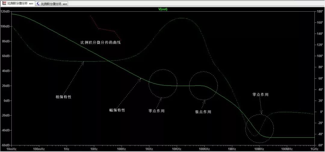
Transfer Function Curve
By looking at the first, second, and third-order transfer function characteristic curves, as well as the transfer function curves of PI, PD, and PID control circuits, it can be understood that feedback control is merely used to correct the phase and amplitude changes in the system caused by inductive and capacitive inertial components due to frequency effects.
To put it simply, it is about correcting the phase and amplitude deviations of the circuit system by introducing operational amplifier compensation circuits. The introduced operational amplifier compensation circuit must ensure sufficient phase margin and gain margin.
As for the poles and zeros we often discuss, they are merely those nodes that significantly influence the phase-frequency and amplitude-frequency characteristics.
I have organized the transfer function curves of the conventional third-order compensation network and PID, and next, I will discuss practical simulation applications, taking the buck power supply as an example.
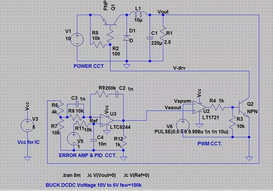
PID-buck Power Supply Circuit
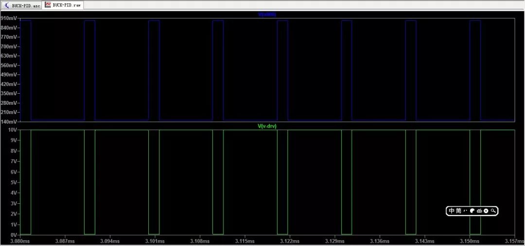
Buck Power MOSFET Drive
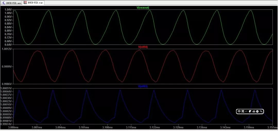
Buck-Feedback Node Waveform
* This article is an original article from the 21Dianyuan community and is prohibited from being reproduced without authorization. Please respect intellectual property rights; otherwise, we reserve the right to pursue responsibility.

Recommended Reading ▼
Analysis of MOSFET Drive Circuits
Discussing the causes and countermeasures of reverse voltage spikes in self-inductance topology based on 5KW
Magnetic Devices and Volt-Second Balance
Further Discussion on High Voltage Integrated Driver ICs
Making an Ultra-Small Power Supply: Learning QR Principles
★ Bookmark 21Dianyuan to learn more information ▼

Let the editor know if you are “watching”