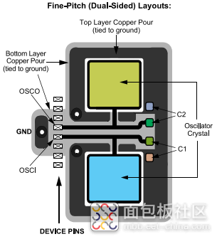
Before we begin: 1. This article will focus on Microchip’s products. I believe Microchip has the most articles on clocks among MCU companies. The terminology used by Microchip may differ from that of other companies, but the usage is the same and does not affect understanding. 2. The term “clock source” is used to distinguish it from the “clock” generated by the internal clock division of the MCU.General-purpose MCUs allow the use of external clock sources. To provide more convenience for MCU applications, the frequency range of external clock sources is generally wide. However, frequency is only one of the three factors in selecting and designing external clock source components, and the remaining two factors will be introduced later.Types of External Clock Sources— Active clock sources: square wave or sine wave input, referenced to Vss. Common examples are crystal oscillators or crystals. — Passive clock sources: components that must be driven by an oscillation circuit, such as various resonators and crystals, which are cheaper. Among them, resonators require more power than crystals. Pin XIN and Pin XOUT X is understood as a homophone for Crystal; IN means input and OUT means output. There is actually an oscillation circuit between XIN and XOUT, called the Pierce parallel resonant oscillator, as shown in the schematic below. The diagram includes an inverter, and the output is fed back to the input through feedback resistor RF, forming an unstable circuit. After connecting an external crystal and resonance capacitors, this circuit will stabilize at unit gain and oscillate at the frequency corresponding to that unit gain. The part within the upper rectangular box in the figure is implemented on the MCU chip.
 (Image from Ref 1) The XIN pin must always be connected, while the XOUT pin is only used when a passive clock source is employed. When using an active clock source, such as a crystal oscillator or an external signal generator, the reference point for the signal source is the MCU’s Vss. In this case, the oscillator inside the MCU is not needed, so only the XIN pin needs to be connected, and the XOUT pin can be left floating or reused for other functions. When using a passive clock source, such as a crystal or resonator, it cannot generate an oscillation signal on its own and requires the built-in oscillation circuit of the MCU. In this case, besides the XIN pin, the XOUT pin must also be used. Below are several application points worth noting when both XIN and XOUT pins are used. 1. Choose the Oscillation Circuit Drive Mode The appropriate drive mode should be selected based on the power requirements of the clock source. As mentioned earlier, among passive external clock sources, resonators require higher drive power compared to crystals. For crystals, AT-Cut crystals require higher drive power compared to low-frequency crystals (e.g., fork-structure 32.768kHz crystals). Therefore, general-purpose MCUs not only have built-in oscillation circuits but also design different drive power modes for the oscillation circuit, such as LS mode, XT mode, and HS mode, with power increasing accordingly. In addition to considering the power requirements of the clock source, attention should also be paid to the power supply voltage of the oscillation circuit, which is often the power supply voltage of the MCU. If the voltage of the oscillation circuit is insufficient, its output power will also decrease (current increase is limited by chip wiring). For example, if the power supply range of an MCU is 1.8~5.0V, but the XT mode of the oscillation circuit is only effective at 3.0~5.0V. If the external power supply drops below 3.0V, the external clock source may stop oscillating. Moreover, such a circuit operates normally above 3.0V, but when switching to low power consumption at 1.8/2.5V, it may not work. 2. Do Not Overdrive The previous discussion addressed oscillation stoppage due to insufficient drive power; now we discuss crystal fatigue or even breakage caused by excessive driving. As described in Basic Theory Article 006, the crystal acting as the clock source operates on the piezoelectric effect. If the voltage provided by the drive circuit is too high, the amplitude of the crystal will be too large, shortening its lifespan or even causing immediate damage, creating reliability risks. 3. Check the Clock Signal How can we determine if the MCU’s external clock source is “suitable”? This brings us to the correct measurement methods. It is recommended to use a high input impedance oscilloscope probe (100:1) to measure the signal at XOUT. This signal should be a low-distortion sine wave. When checking with a regular voltage probe, the capacitance of the probe itself may change the characteristics of the oscillation circuit, causing it to stop oscillating. — If the waveform is clipped or has a high distortion rate, the drive power of the oscillation circuit should be immediately reduced, for example, from HS to XT. — If reducing to XT still does not completely resolve the issue, a resistor should be connected in series with the crystal to dissipate excess power, as shown in the above figure with R1. — If the oscillation signal does not operate at the required frequency but at some multiple or divided frequency, it also indicates that the drive power is not suitable and needs immediate adjustment. Finally, such checks should be conducted at all stages of development, whether it is the initial functional prototype or the process prototype. If the PCB design is modified or the crystal is changed, it is even more necessary to check. Now, let’s briefly summarize the PCB wiring considerations. The oscillation circuit formed between the external clock source and the MCU is detrimental to weak signal conditioning and EMC. Therefore, it should be treated with high-frequency circuit considerations in mind for PCB wiring. First, keep the circuit loop small. The external clock source, such as a crystal, should not be more than 15mm from the XIN/XOUT pins, ideally 10~12mm. This distance avoids DFA issues. Choose small form factor products for the crystal, capacitors, and resistors. Second, implement electrical shielding. Surround the oscillation circuit on the PCB with a grounded (or other fixed potential) conductor to form a Guard Ring, and then ground one point of the shield ring. For metal-encased crystals, a wire can be soldered from the metal shell to the PCB ground, providing electrical shielding. For general-purpose MCUs with many pins, there is usually a Vss pin arranged next to the XIN/XOUT pins, which is the best location for grounding one point of the shield ring. MCUs with fewer pins may not have this pin, so consider connecting to the single point where the analog ground meets the digital ground. Lastly, avoid coupling. Do not arrange other lines in the area of the oscillation circuit. For double-sided and multi-layer PCBs, consider opening copper skin windows under the oscillation circuit; below is a wiring example:
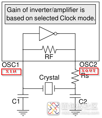
 (Image from Ref2, single-sided board with dual crystals)
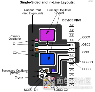
(Image from Ref2, double-sided board with a single crystal) Ref1. DS00838A. Basic PIC16/17 Oscillator Design. Microchip 2. Guidelines for Getting Started with PIC18-Q71 Microcontrollers – 4.5 External Oscillator Pins. Microchip 3. DS00949A. Making Your Oscillator Work. MicrochipAuthor: Blog Contributor from Breadboard Community Electronic Knowledge Sharing
(Image from Ref2, single-sided board with dual crystals)
(Image from Ref2, double-sided board with a single crystal) Ref1. DS00838A. Basic PIC16/17 Oscillator Design. Microchip 2. Guidelines for Getting Started with PIC18-Q71 Microcontrollers – 4.5 External Oscillator Pins. Microchip 3. DS00949A. Making Your Oscillator Work. MicrochipAuthor: Blog Contributor from Breadboard Community Electronic Knowledge Sharing
Free Application for Development Board

For submissions/promotions/collaborations/joining the group, please scan the QR code to add WeChat
(Please specify your intention, and if joining the group, please specify city – name – industry position information)

Exciting Surprises at the Exhibition!Join the Disassembly Event! Get Development Boards on-site!👇 Hurry Up and Sign Up!