As part of the “2022 Research and Analysis Report on 45 Domestic AI Chip Manufacturers”, the AspenCore analyst team compiled a list of 10 domestic AI chips and 10 international AI chips to showcase the latest technological developments in global AI chips.
The top 10 domestic AI chips come from the following manufacturers: Cambricon, Horizon Robotics, Kunlun Core Technology, Alibaba T-Head, Suirian Technology, Hanbo Semiconductor, Tensyn, Kunyun Technology, Hezhima Intelligent, and Xinqing Technology. (Please vote for your favorite domestic AI chip at the end of the article.)
The top 10 international AI chips come from the following manufacturers: NVIDIA, Intel, Google, AWS, Qualcomm, Esperanto, Graphcore, Cerebras, Ambarella, and Hailo.
During the research and compilation process of the “AI Chip” report, the processor IP leader Arm Technology, domestic EDA company Hejian Technology, and leading domestic AI chip design company Hanbo Semiconductor provided great support, for which we express our sincere gratitude! Additionally, Mr. Wu Xiongang, Chairman of Arm Technology, and Ms. Xu Yun, Co-President of Hejian Technology, will participate in the Shanghai IIC exhibition and give keynote speeches at the IC Leaders Summit.
Scan the QR code below to register

Top 10 Domestic AI Chips
Cambricon Third-Generation Cloud AI Chip Siyuan 370
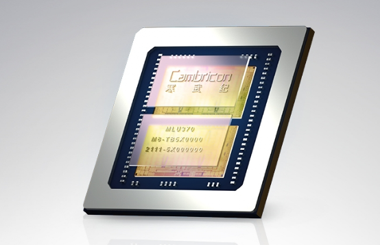
The Siyuan 370 is based on a 7nm process, integrating 39 billion transistors and utilizing chiplet technology, with a maximum computing power of 256 TOPS (INT8), which is twice that of Siyuan 270. Based on the latest intelligent chip architecture MLUarch03, the Siyuan 370 combines AI training and inference, demonstrating excellent performance: for instance, the MLU370-S4 accelerator card (half-height half-length) has a measured performance that is twice that of mainstream GPUs of the same size; the MLU370-X4 accelerator card (full-height full-length) has performance comparable to mainstream GPUs of the same size, with significantly better energy efficiency.
The Siyuan 370 packages two AI computing chiplets (MLU-Die) on a single chip, with each MLU-Die featuring independent AI computing units, memory, I/O, and MLU-Fabric control and interfaces. The MLU-Fabric ensures high-speed communication between the two MLU-Dies, while different combinations of MLU-Dies can achieve diverse products, providing users with cost-effective AI chips suitable for various application scenarios.
Horizon Robotics Vehicle Intelligent Computing Platform Journey 5
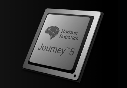
The Journey 5 is Horizon Robotics’ third-generation automotive-grade AI chip, developed using TSMC’s 16nm FinFET process, following the ISO 26262 functional safety certification process, and has passed ASIL-B certification. Based on the latest dual-core BPU Bayesian architecture design, Journey 5 employs an octa-core Arm Cortex-A55 CPU cluster, providing up to 128 TOPS equivalent computing power; CV engine, dual-core DSP, dual-core ISP, and powerful Codec; supports multiple 4K and full HD video inputs and processing; dual-core lock-step MCU, achieving ASIL-B(D) functional safety level; complies with AEC-Q100 Grade 2 automotive grade standards.
This chip is aimed at high-level autonomous driving and intelligent cockpit applications, with rich external interfaces capable of connecting over 16 channels of HD video input and supporting dual-channel “instant” image processing; leveraging BPU, DSP, and CPU resources, it is suitable for advanced image perception algorithm acceleration and can also support multi-sensor fusion such as LIDAR and millimeter-wave radar; features PCIe 3.0 high-speed signal interface, dual-channel gigabit real-time Ethernet (TSN) providing hardware-level support for multi-sensor synchronous fusion (PTP); supports predictive planning and H.265/JPEG real-time encoding and decoding.
Kunlun Core Generation 2
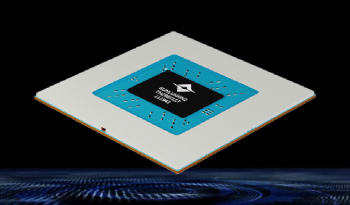
The second generation of cloud universal AI chips launched by Kunlun Core Technology, which was independently established from Baidu’s Intelligent Chip and Architecture Department, uses a 7nm process and is based on a new generation of self-developed XPU-R architecture, with computing power of 256 TOPS@INT8, 128 TFLOPS@XFP16/FP16, and a maximum power consumption of 120W; supports GDDR6 high-performance video memory; highly integrated ARM CPU, supporting encoding and decoding, inter-chip interconnection, security, and virtualization.
In hardware design, this chip is the first universal AI chip to use video memory. In software architecture, Kunlun 2 has significantly iterated the compiler engine and development suite, supporting C and C++ programming. Additionally, Kunlun 2 has completed end-to-end adaptation with several domestic general processors such as Feiteng, various domestic operating systems such as Kirin, and Baidu’s self-developed PaddlePaddle deep learning framework, possessing full-stack domestic AI capabilities in software and hardware. This chip is applicable in various scenarios including cloud, edge, and can be utilized in fields such as core internet algorithms, smart cities, smart industry, and will also empower high-performance computing clusters, biological computing, intelligent transportation, and autonomous driving in broader spaces.
Alibaba T-Head Hanguang 800
T-Head released the data center AI inference chip Hanguang 800 in 2019, based on a 12nm process, integrating 17 billion transistors, with a peak performance computing power of 820 TOPS. In the industry-standard ResNet-50 test, the inference performance reached 78563 IPS, with an energy efficiency ratio of 500 IPS/W.
Hanguang 800 adopts the self-developed architecture of T-Head, achieving performance breakthroughs through collaborative design of software and hardware. The self-developed AI chip software development kit allows Hanguang 800 to achieve high throughput and low latency high-performance experience when developing deep learning applications. Hanguang 800 has been successfully applied in scenarios such as data centers and edge servers.
Suirian “Suis” 2.5 Cloud AI Inference Chip
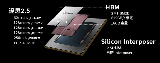
The Suis 2.5 AI inference chip is based on the second-generation GCU-CARA architecture, serving as the computing core of the Cloud Suis i20 high-performance inference card, featuring a large chip size of 55mm × 55mm, providing full precision AI computing power from single precision floating-point to INT8; based on HBM2E storage solutions, providing 819GB/s storage bandwidth; with hardware-based power consumption monitoring and optimization features, achieving a 3.5X energy efficiency improvement. This chip can support model inference for various applications including vision, speech, NLP, search, and recommendation.
The new generation “Suis” AI inference chip adopts a 12nm process, significantly improving transistor efficiency per unit area through architectural upgrades, achieving computing power comparable to current 7nm GPUs in the industry. The cost advantages brought by the mature 12nm process make the Cloud Suis i20 accelerator card more cost-effective under the same performance.
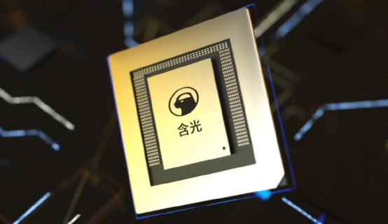
Hanbo Semiconductor AI Inference Chip SV100
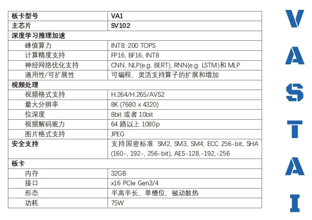
The SV100 series chips (SV102) are positioned as general-purpose AI inference chips for the cloud, characterized by high inference performance (single chip INT8 peak performance of 200 TOPS, also supporting FP16/BF16 data types), low latency, and video decoding performance supporting 64+ channels of 1080p (decoding formats support H.264, H.265, AVS2).
The SV102 chip has a dedicated hardware video decoding unit, whose video processing and deep learning inference performance metrics are several times higher than existing mainstream data center GPUs. Based on Hanbo’s self-developed general architecture optimized for various deep learning inference loads, this chip can support AI inference application scenarios such as computer vision, video processing, natural language processing, and search recommendation, while integrating high-density video decoding, widely applicable to cloud and edge solutions, saving equipment investment and reducing operating costs.
Tensu Intelligence GPGPU Cloud Training Chip
The Tensu Intelligence cloud training chip BI, based on a fully self-developed GPGPU architecture, adopts TSMC’s 7nm process, integrating 24 billion transistors, and employs 2.5D CoWoS wafer packaging technology. This chip supports mixed training with multiple precision data types including FP32, FP16, BF16, INT8, and supports inter-chip interconnection, with a single-chip computing power of up to 147T@FP16.
Through a rich self-developed instruction set, this chip can support scalar, vector, and tensor operations, efficiently supporting various high-performance computing through programmable and configurable features. This GPGPU chip focuses on high performance, generality, and flexibility, providing matching computing power for the rapidly developing AI and related vertical application industries, and solving the pain points of product usability and high migration costs of development platforms through standardized software and hardware ecosystems.
Kunyun Technology Data Stream AI Chip CAISA
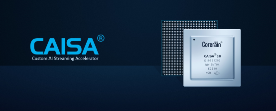
The CAISA chip adopts Kunyun’s self-developed custom data stream architecture CAISA 3.0, which has significantly improved efficiency and measured performance compared to the previous generation chip architecture. CAISA 3.0 provides 4 times the parallelism options in multi-engine support, greatly enhancing the scalability of the architecture. Within the AI chip, each CAISA can simultaneously handle AI workloads, achieving a peak computing power increase of 6 times while maintaining a chip utilization rate of up to 95.4%. In addition, this chip supports a more general operator support, enabling rapid implementation of detection, classification, and semantic segmentation deployment for the vast majority of neural network models.
Kunyun has achieved a technological breakthrough in measured chip computing power through its self-developed data stream technology, with chip utilization exceeding 95%, improving by up to 11.6 times compared to similar products. This customized data stream technology does not rely on advanced wafer manufacturing processes and larger chip areas, but rather enhances measured performance by controlling the order of computation through data flow, providing users with higher computing power cost-effectiveness.
Hezhima Intelligent Autonomous Driving Chip Huashan No. 2 A1000 Pro
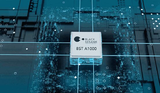
The Hezhima Intelligent A1000 Pro adopts a 16nm process, with a single chip INT8 computing power of 106 TOPS and INT4 computing power of 196 TOPS, with a typical power consumption of 25W, meeting the ISO 26262 ASIL D-level functional safety requirements. A1000 Pro has a built-in high-performance GPU, capable of supporting high-definition 360-degree 3D panoramic image rendering, and can be configured with different data paths and computing mechanisms, deploying mutually redundant dual systems and safety island verification internally.
Based on one, two, or four A1000 Pros, Hezhima’s FAD fully autonomous driving platform can meet the computing power requirements for L3/L4 autonomous driving functions, supporting automatic driving scenarios from parking, urban roads to highways.
Xinqing Technology “Long Eagle No. 1” Intelligent Cockpit Chip
The Xinqing Technology 7nm automotive-grade intelligent cockpit multimedia chip “Long Eagle No. 1” is produced by TSMC, integrating “one chip multi-screen multi-system” for the intelligent cockpit, incorporating voice recognition, gesture control, LCD instrument, HUD, DMS, and ADAS fusion functions, allowing drivers to enjoy a more intuitive and personalized interactive experience.
“Long Eagle No. 1” features 8 CPU cores, 14 GPU cores, and an 8 TOPS INT 8 programmable convolutional neural network engine. This chip reaches AEC-Q100 Grade 3 level, adopting a safety island design that meets ASIL-D standards, with an independent Security Island information security island built-in, providing a high-performance encryption and decryption engine, supporting national encryption algorithms such as SM2, SM3, SM4, and supporting secure boot, secure debugging, and secure OTA updates. Powerful CPU, GPU, VPU, ISP, DPU, NPU, and DSP heterogeneous computing engines, along with high-bandwidth low-latency LPDDR5 memory channels and high-capacity external storage, provide comprehensive computing power support for intelligent cockpit applications.
Top 10 International AI Chips
NVIDIA A100 Tensor Core GPU
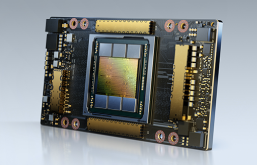
The NVIDIA A100 Tensor Core GPU is based on the NVIDIA Ampere architecture, offering two configurations of 40GB and 80GB. As the engine of NVIDIA’s data center platform, the A100’s performance has improved by up to 20 times compared to the previous generation, and can be partitioned into seven GPU instances for dynamic adjustments based on changing demands. The A100 excels in AI, data analysis, and HPC application scenarios, achieving outstanding acceleration at different scales, effectively supporting high-performance elastic data centers.
For deep learning training, the A100’s Tensor Core offers up to 20 times the performance of the previous generation NVIDIA Volta, thanks to Tensor floating-point operations (TF32) precision, without requiring code changes; using automatic mixed precision and FP16 can further enhance performance by 2 times. 2048 A100 GPUs can process large-scale training workloads like BERT in under a minute. For ultra-large models with extensive data tables (e.g., DLRM for recommendation systems), the A100 80GB provides up to 1.3TB of unified memory per node, and can be up to 3 times faster than the A100 40GB.
For deep learning inference, the A100 can accelerate across the entire precision range from FP32 to INT4. The Multi-Instance GPU (MIG) technology allows multiple networks to run simultaneously on a single A100, optimizing the utilization of computing resources. On top of the performance gains for inference, structured sparsity support alone can yield up to double the performance improvement.
Intel Neuromorphic Chip Loihi 2
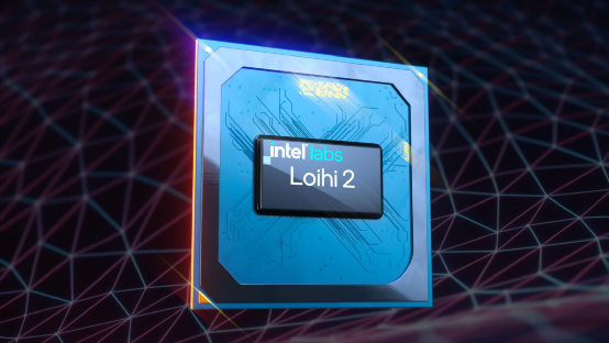
The second generation neuromorphic chip Loihi 2 released by Intel has an area of 31mm, capable of packaging up to 1 million artificial neurons, compared to the previous generation’s 60mm area supporting 131,000 neurons. Loihi 2 operates at speeds 10 times faster than the previous generation, with a resource density increase of 15 times and improved energy efficiency. Loihi 2 features 128 neuromorphic cores, each with 8 times the number of neurons and synapses compared to the first generation, interconnected by 120 million synapses.
Loihi 2 uses a more advanced manufacturing process—Intel’s first EUV process node, Intel 4, now requiring only half the space previously needed per core. Additionally, Loihi 2 can communicate between chips through a 2D mesh and also communicate on a 3D scale, greatly increasing the total number of neurons that can be processed. The number of embedded processors per chip has increased from three to six, and the number of neurons per chip has increased eightfold.
The Loihi 2 neuromorphic chip can effectively solve many problems using Spiking Neural Networks (SNN), but the current difficulty lies in the fact that this very different programming type requires thinking about algorithm development in a similarly different way. Most of those proficient in it come from theoretical neurobiology, and limiting Loihi 2 to research fields will restrict its market sales scope. Intel hopes to combine Loihi 2 with the open-source software framework Lava, aiming for Loihi derivatives to eventually appear in a wider range of systems, from co-processors in embedded systems to large Loihi clusters in data centers.
Google TPU 4
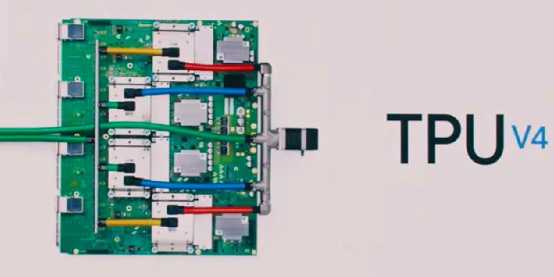
The fourth-generation AI chip TPU v4 from Google reaches speeds 2.7 times that of TPU v3. By integrating 4096 TPU v4 chips into a single TPU v4 Pod, it can achieve exaflop-level computing power, equivalent to 10 million laptops combined, and double that of the world’s first supercomputer, Fugaku. In addition to using these systems for its own AI applications (such as search suggestions, language translation, or voice assistants), Google also offers TPU infrastructure as a cloud service (for a fee) to Google Cloud users.
The matrix multiplication TFLOP provided by the fourth-generation TPU is more than double that of TPU V3, significantly improving memory bandwidth. The performance of TPU v4 pods has improved by 10 times compared to TPU v3 pods, and will primarily operate on carbon-free energy, not only computing faster but also being more energy-efficient.
AWS Trainium Cloud Inference Chip
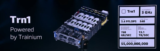
AWS’s second custom machine learning chip, AWS Trainium, is specifically optimized for deep learning training workloads, including image classification, semantic search, translation, speech recognition, natural language processing, and recommendation engines, while supporting TensorFlow, PyTorch, and MXNet. Compared to standard AWS GPU instances, EC2 TRN1 instances based on this chip have a 30% increase in throughput, reducing model inference costs by 45%.
AWS Trainium shares the same AWS Neuron SDK as AWS Inferentia, making it easy for developers using Inferentia to start using Trainium. AWS Trainium will be provided through Amazon EC2 instances, AWS deep learning AMIs, and managed services (including Amazon SageMaker, Amazon ECS, EKS, and AWS Batch).
Qualcomm Cloud AI100
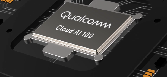
The Qualcomm Cloud AI 100 inference chip uses a 7nm process, containing 16 AI cores, with an INT8 inference throughput of 400 TOPS, and a memory controller for 4 channels @ 64-bit LPDDR4X-4200 (2100MHz), with a total system bandwidth of 134 GB/s.
Qualcomm provides three different packaging forms for commercial deployment, including a mature PCIe 4.0 x8 interface, as well as DM.2 and DM.2e interfaces (25W / 15W TDP), with power consumption as follows: DM.2e @ 15W, DM.2 at 25W, PCIe/HHHL @ 75W.
Esperanto ET-SoC-1
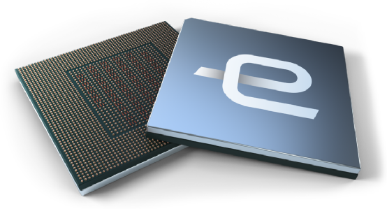
The Esperanto ET-SoC-1 chip, based on RISC-V, integrates 1000 cores and is designed for data center AI inference. This chip is manufactured using TSMC’s 7nm process, built-in 160M BYTE SRAM, and contains 24 billion transistors.
The ET-SoC-1 core includes 1088 ET-Minions and 4 ET-Maxions. ET-Minions are general-purpose 64-bit orderly cores with proprietary extensions for machine learning, including vector and tensor operations of up to 256 bits per clock cycle. ET-Maxion is the company’s proprietary high-performance 64-bit single-thread core, using quad-issue out-of-order execution, branch prediction, and prefetching algorithms.
Graphcore IPU Colossus Mk2 GC200
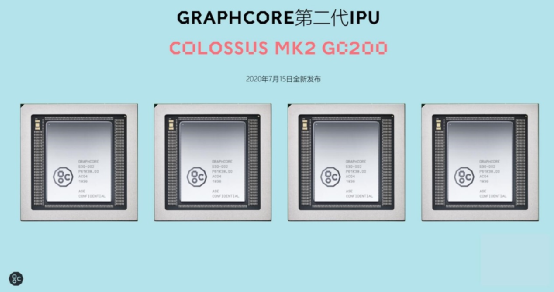
The second-generation IPU chip Colossus MK2 GC200 from Graphcore adopts TSMC’s 7nm process, with architecture similar to the previous generation IPU, but the number of cores has increased to 1472 (an increase of 20%), and its on-chip SRAM has increased to 900MB (three times more). In terms of interconnect scalability, it has been enhanced 16-fold compared to the previous generation.
The system solution containing four MK2 chips, IPU-M2000, can scale up to 1024 IPU-PODs, i.e., 512 racks, with up to 64000 MK2 chips clusters, achieving 16 ExaFLOPs of 16-bit FP computing power. The M2000 device contains a Gateway chip that provides access to DRAM, 100Gbps IPU-Fabric Links, PCIe interfaces connected to SmartNICs, 1GbE OpenBMC management interfaces, and M.2 interfaces. The performance of M2000 in neural network training is 7-9 times that of the previous generation, and inference performance has improved by over 8 times.
Cerebras WSE-2
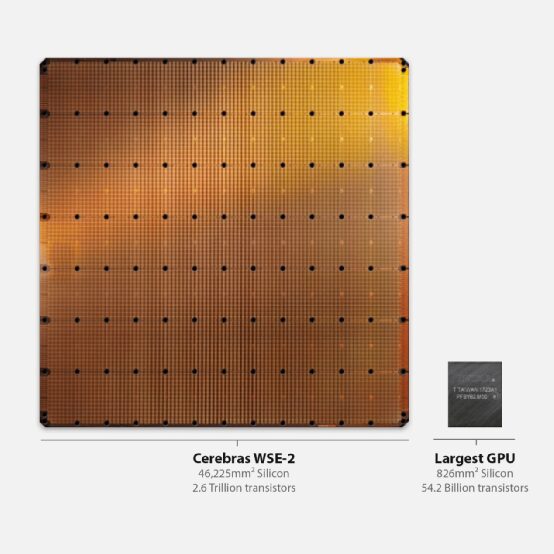
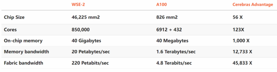
The largest chip ever designed and manufactured by Cerebras is called the Wafer Scale Engine (WSE), and the second-generation chip WSE-2 uses TSMC’s N7 process, with an area of 46225mm2, containing over 1.2 trillion transistors, and 850,000 cores fully optimized for deep learning. Compared to the NVIDIA A100 GPU, WSE is over 56 times larger, with on-chip memory reaching 40GB, memory bandwidth of 20PB/s, and network bandwidth of 220PB/s.
The AI acceleration system based on WSE-2, CS-2, significantly increases memory and architectural bandwidth while maintaining its system power consumption at 23kW. The computing processing performance of a single CS-2 system is equivalent to dozens or hundreds of GPUs, reducing the time required to complete the most complex AI workloads from months to minutes.
Ambarella CV52S

Based on the Ambarella CVflow architecture and advanced 5nm process, the CV52S single SoC features ultra-low power consumption while supporting 4K encoding and powerful AI processing. This chip features a dual-core 1.6GHz Arm A76, with 1MB L3 cache; powerful ISP with excellent wide dynamic range, low light, fisheye correction, and rotation processing performance; built-in privacy masking feature to obscure parts of the captured scene; new PCIe and USB 3.2 interfaces for more complex multi-chip security system designs; supports secure boot, OTP, and Arm TrustZone for robust hardware-level digital security, ensuring the information security of security camera devices; supports multi-channel video stream input, capable of connecting up to 14 cameras via MIPI virtual channel interfaces; supports LPDDR4x/LPDDR5/LPDDR5x DRAM.
Compared to the previous generation chip, the CV52S series chips aimed at single-lens security cameras support 4K60fps video recording, while AI computer vision performance has increased by 4 times, CPU performance has doubled, and memory bandwidth has increased by over 50%. Improvements in neural network (NN) performance allow for more types of AI processing to be executed on edge devices without needing to upload to the cloud.
Hailo Edge AI Processor Hailo-8
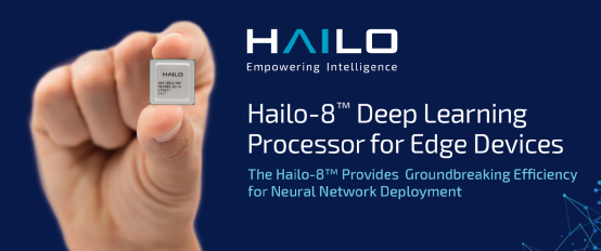
The Hailo-8 edge AI processor from Israeli AI chip company Hailo achieves a performance of 26 tera operations per second (TOPS), with an efficiency of 2.8 TOPS/W. According to the company, the Hailo-8 outperforms Nvidia’s Xavier AGX, Intel’s Myriad-X, and Google’s Edge TPU module in multiple AI semantic segmentation and object detection benchmark tests.
The M.2 module based on Hailo-8 is a dedicated accelerator module for AI applications, providing up to 26 TOPS of computing power, suitable for edge computing, machine learning, and inference decision-making applications. The M.2 module has a complete PCIe Gen-3.0 4 channel interface, which can be inserted into existing edge devices with M.2 sockets for real-time, low-power deep neural network inference, applicable to a wide range of niche markets.