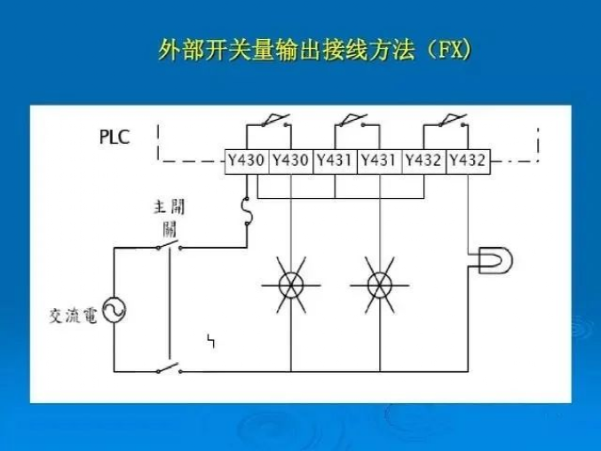
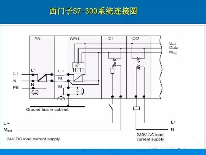
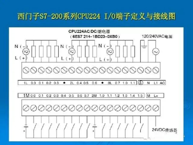
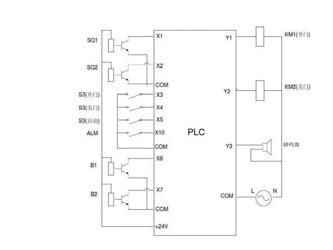
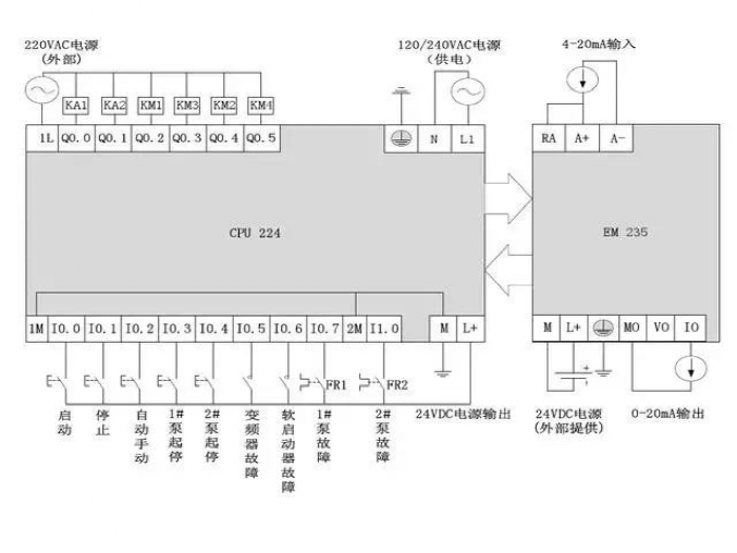
PLC automation control is widely used in electrical automation and intelligent control, which is well known among personnel in the electrical industry. In addition to requiring the input of predefined programs, PLC automation control also requires wiring for input and output ports of the PLC itself. Only when the program instructions of the PLC are correct, and the wiring for input and output ports is correct, can the PLC perform automation control. Experienced engineers know that PLCs can accept both digital control and analog control, and the two can be converted into each other. Today, we will focus on the external wiring of the PLC and how digital signals and analog signals are converted!
External Wiring of PLCs — Wiring Methods
• Common Point Type…… Each I/O circuit has a common point, sharing a single power supply.
• Group Type…… I/O is divided into several groups, with each group sharing a power supply, and each group can have different power supplies.
• Isolated Type…… Each I/O point is isolated from each other, and each I/O can use an independent power supply.
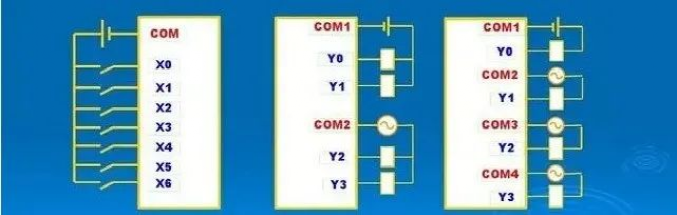
External Wiring of PLCs — Input Modules
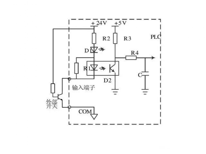
Function of Input Interfaces: To convert signals generated by buttons, limit switches, or sensors into digital signals sent to the main unit.
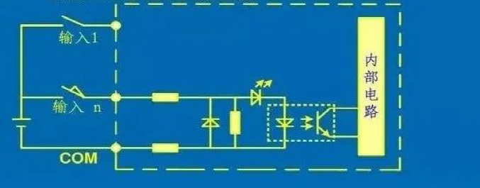
Isolation circuits use optocouplers, and then through RC filter circuits, the signals are sent to the PLC’s CPU, which can prevent external interference and contact bounce.
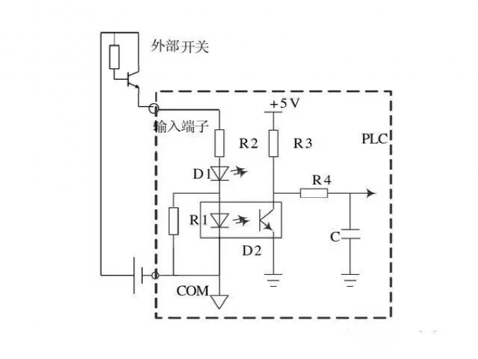
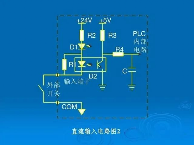
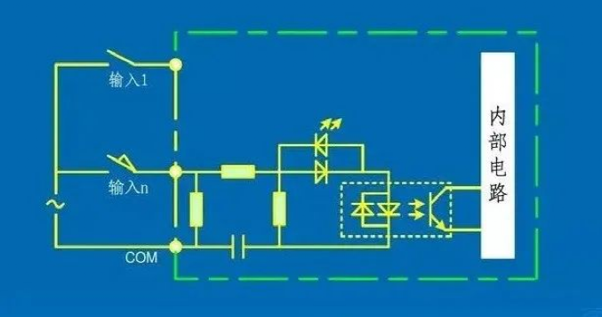
Light-emitting diodes and optocouplers use reverse connection configurations, allowing AC input to pass through the positive and negative half waves separately, with C1 serving as a rectifier.
External Wiring of PLCs — Output Modules
1) Relay Output: Low-speed, high-power
DC and AC loads (isolation, power amplification)
2) Transistor Collector Output: High-speed, low-power
DC loads
3) Bidirectional Thyristor Output: High-speed, high-power
AC loads
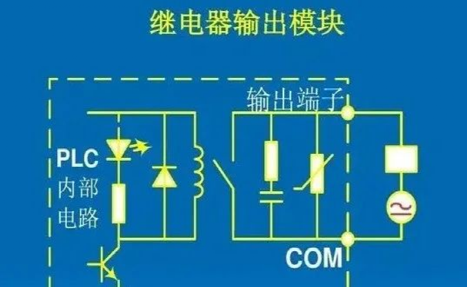
Response speed is less than 10ms, mainly due to the mechanical contact operation delay. The load power supply is provided externally, and the RC circuit connected to the contacts is used to eliminate load current generated when the contacts open.
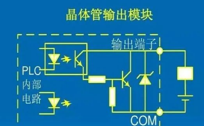
Amplification uses high-power transistors or field effect transistors, with response speeds less than 1ms. The transistors operate in saturation and cutoff states, and the voltage regulator diode in the diagram is used to suppress overvoltage during shutdown.
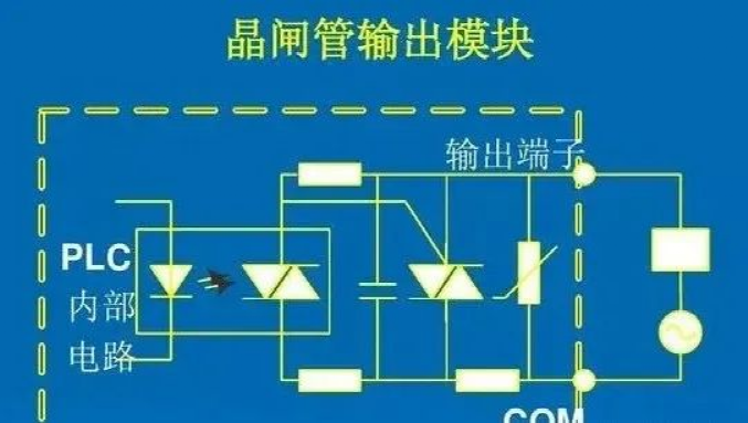
Isolation uses optocouplers, amplification uses bidirectional thyristors, and the response time has two scenarios: the delay time for the thyristor to switch from off to on is less than 1ms, and the delay time for switching from on to off is less than 10ms. The RC circuit and voltage-sensitive resistors are used to suppress overvoltage during thyristor shutdown and external surge voltages.
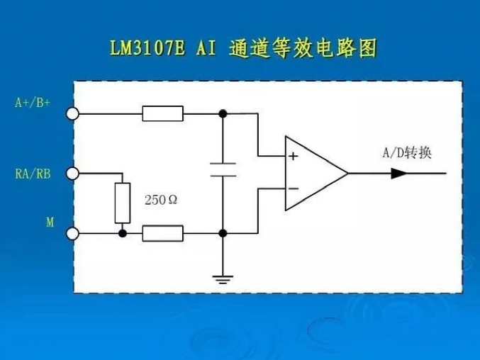
Analog Input Modules (A/D, AI)
A/D Function: Converts the (standard) analog signals output by field instruments, such as 4-20mA, 0-10VDC, into digital signals that can be processed by computers.
A/D Conversion Performance Indicators
Resolution *—— A/D interface converts one LSB (Least Significant Bit) when the minimum change of the input analog signal occurs. For example: a 12-bit A/D converter with an input range of 0-10VDC, the resolution = 10/2^12 = 2.44mV.
(Resolution is usually expressed in terms of the number of bits of the input binary number: 10 bits, 12 bits resolution) Linearity Error — The maximum deviation between the actual conversion characteristic curve and the ideal conversion characteristic curve.
Includes: Offset Error (0 input not equal to 0 output), Non-linearity Error, etc. Linearity error is usually expressed as a fraction of LSB: e.g., ±1/2 LSB, ±1 LSB, etc.
Conversion Time *—— The time required from the start of conversion to the completion of one A/D conversion.
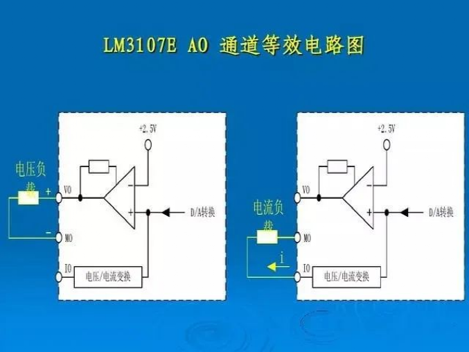
Analog Output Modules (D/A, AO) D/A Function: Converts internal digital signals from the computer into standard signals that can be received by field instruments, such as 4-20mA. For example: a 12-bit digital value (0-4095) → 4-20mA; 2047 corresponds to the conversion result: 12mA.
D/A Conversion Performance Indicators
Resolution — The minimum change in the analog output signal when one LSB (Least Significant Bit) is converted (usually resolution is expressed in terms of the number of bits of the input binary number: 10 bits, 12 bits D/A converters) Linearity Error — The maximum deviation between the actual conversion characteristic curve and the ideal conversion characteristic curve, including offset error (0 input not equal to 0 output), Non-linearity Error, etc.
Linearity error is usually expressed as a fraction of LSB: e.g., ±1/2 LSB, ±1 LSB, etc. Establish Time — The time taken for the output analog signal to stabilize within the specified range (±0.5xLSB).
Disclaimer: This article is a network reprint or adaptation, and the original author could not be found. Copyright belongs to the original author. If there are copyright issues, please contact for deletion.