Description
I2C supports N-2-N on the bus, so addresses are needed to distinguish devices.
A complete transmission always starts with a START signal followed by the device address and the read/write flag.
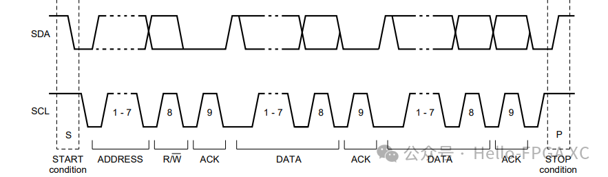
Device Address
So how do we view and define the device address?
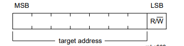
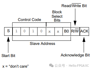
The device address corresponds to the first BYTE’s BIT7-BIT1, with BIT 0 corresponding to the read/write flag.
The I2C protocol specifies that all addresses can be used except for 0000 XXX and 1111 XXX.
Example
How can we view the device address based on the hardware schematic?
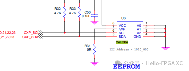
This is a schematic example; the manual specifies that the device address format for the 24LCXX series is 1010 XXX, where XXX corresponds to the values of A2, A1, and A0 in the hardware schematic. Therefore, the actual I2C address corresponding to the current schematic is 1010 000, which corresponds to 0X50.
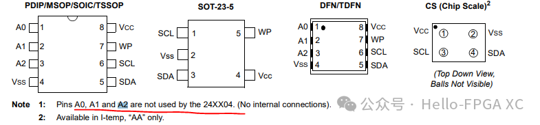
However, please note that the 24LC04 corresponds to an EEPROM storage capacity of 4Kb, 512 bytes, and accessing all addresses requires at least a 9-bit address space. Therefore, the lowest address BIT of the device is used for BLOCK selection, which is used to extend the address width.
The last bit, B0, is used by the master
device to select which of the two 256-word blocks of
memory are to be accessed. This bit is, in effect, the
Most Significant bit of the word address.
The current schematic shows that A2, A1, and A0 are grounded. Since the chip does not use these pins, it should have no effect.
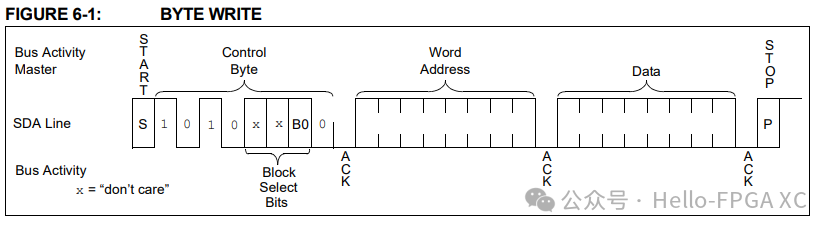
Typical timing for writing a word operation
https://www.nxp.com.cn/docs/en/user-guide/UM10204.pdf
https://ww1.microchip.com/downloads/en/DeviceDoc/21708K.pdf