

When it comes to flashing firmware, everyone is familiar with it. The essence of flashing is to update all or part of the programs in the chip and external memory of embedded products.
Based on the various methods of programming chips involved from PCB production to R&D debugging, assembly, and finally to the user, today we will discuss and sort out these methods.
Flashing carries risks; please be cautious when flashing.
Online Programming vs. Offline Programming
According to whether the chip is programmed while mounted on the board, it can be divided into offline programming and online programming.
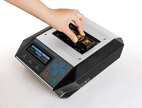
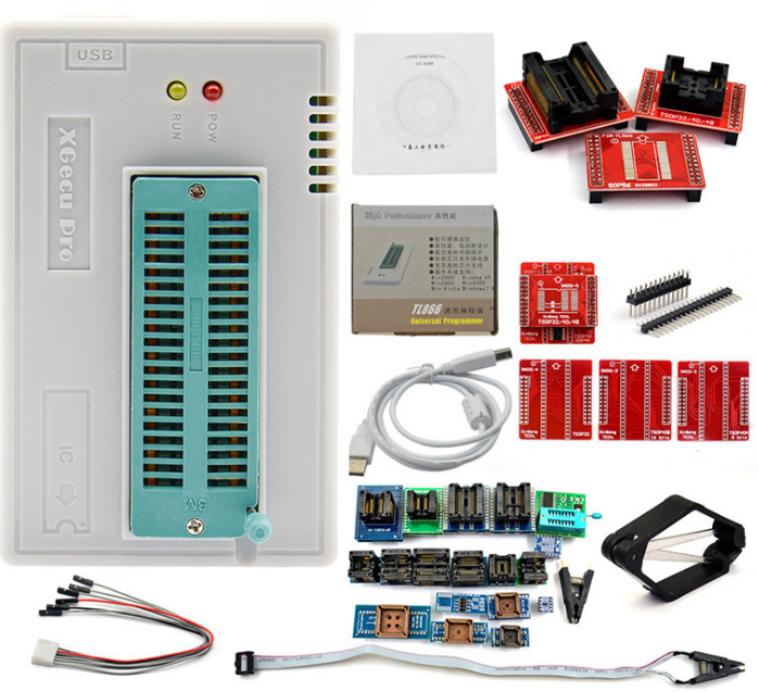
Offline Programming: Usually refers to “bare chip programming.” The MCU chip is programmed on a programmer with the appropriate adapter before being mounted on the PCB. As we know, embedded chips require basic peripheral circuits to function, and programming is no different. Offline programming essentially builds the peripheral circuits and equipment (such as power supply and JLINK) needed for chip programming into an offline programmer. Once the chip is placed in the adapter and powered on, it creates a basic programming environment. By using a PC or some extended functions of the programmer itself, the corresponding program can be programmed. Without considering the time for placing and removing the chip, the programming speed is very fast. The following images are commonly found offline programmers from ZLG and 1688, for reference only.
Online Programming: Usually refers to programming chips that are already mounted on the PCB through various communication interfaces of the chip itself, such as USB, SWD, JTAG, UART, etc. This method is limited by the performance of the serial interface itself; speeds can vary. If using SWD or JTAG, the programming speed is similar to offline programming, but if using UART or similar interfaces, the speed is relatively slower due to baud rate limitations. During product development, programmers download and debug programs using a JLINK box, which is a form of online programming. The image below shows a development board from a certain manufacturer with a JTAG interface.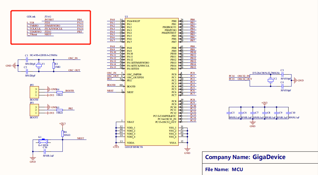
ICP, ISP, IAP
ICP (In Circuit Programming): Programming in the circuit, using the chip’s Debug Access Port for code programming, such as ARM core chips primarily using SWD (Serial Wire Debug) or JTAG (Joint Test Action Group). The offline programming mentioned in section 2 can actually be classified under this method.
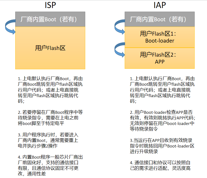
ISP (In System Programming): Programming in the system, which can utilize the bootloader pre-installed by the chip manufacturer to program code through onboard UART, USB, SPI, etc. For example, most STM32 series chips come with a manufacturer-provided bootloader, allowing the MCU to support downloading via UART through ST’s flash-loader on a host computer.
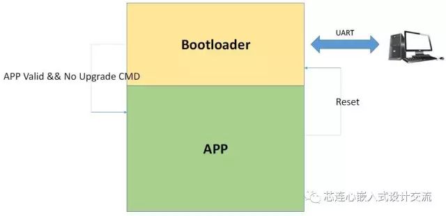
IAP (In Application Programming): Programming in the application, where developers implement the bootloader functionality for programming upgrades. Generally, embedded product software is divided into two parts: the first part is the bootloader, and the second part is the main application (Main APP), which are stored in different areas of flash memory. The bootloader is executed first after power-up or reset, allowing us to initialize some hardware devices, check the integrity of the program, and determine whether to jump from the bootloader to the APP or update the APP. The main program is the one that implements the product functionality aimed at customers. Typically, the bootloader will implement one or more IAP methods, which may include UART, SPI, CAN, or Ethernet, etc. Flashing smartphones and upgrading wearables via Bluetooth fall under this category.
The main differences between ISP and IAP are as follows.
IAP: How to Debug and Simultaneously Program IAP Programs
Continuing on, for IAP, during the development and production phases, we often need to debug or simultaneously program the bootloader and the corresponding main APP programming files.
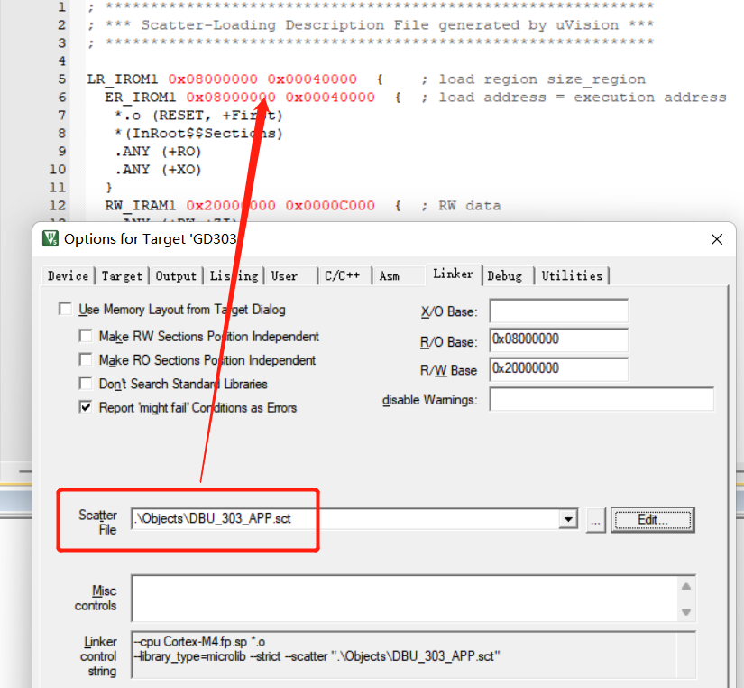
1. First, clarify that the bootloader and Main APP projects have been set up with link files, which will produce programming files with address information during the compilation and linking stages, ensuring no address conflicts.
Taking Keil as an example, you can choose and edit the link file in the Linker.
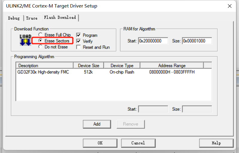
2. Then, in the Debug options, check Erase Sectors, so during debugging and programming, Keil will automatically erase only the areas specified in the link file. This allows for separate programming and debugging of the two projects without interference.
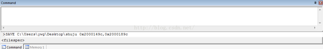
3. After separately programming the bootloader and Main APP programs, you can open the command window in debug mode. See the illustration below.
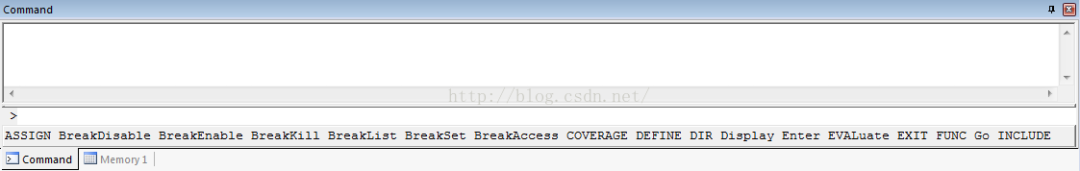
The command window supports exporting data from specified memory areas of the existing chip and saving it as an intel-hex file, allowing us to use this feature to export all code data from the user’s entire Flash area to a hex file, effectively merging the bootloader and Main APP programming files.
The syntax is as follows: SAVE path\filename startAddr, endAddr
4. At the production line, you can use Keil’s tools to program the merged hex file, allowing for simultaneous programming of the bootloader and Main APP, thus improving efficiency.
5. Additionally, J-Flash, STM32 ST-LINK Utility, and Uniflash also have similar functionalities. This will not be elaborated further.