There are many types of ADCs, each with various accuracies and errors. This article will discuss the accuracy and errors related to ADCs.
ADC: Analog Digital Converter, refers to the conversion of analog (voltage) signals into digital signals.
Most MCUs integrate ADC modules, and ADC is a commonly used module in product development. Most people have likely used the ADC function.
In STM32, there are up to four advanced 12-bit ADC controllers (ADC1, 2, 3, 4). Of course, the number of ADC controllers depends on the STM32 model, and some STM32s have 16-bit sampling ADCs (like STM32F373). They provide self-calibration functions to improve ADC accuracy under varying environmental conditions.
When we usually use ADCs, the accuracy requirement may not be high, so we might not focus on whether the ADC conversion values are precise. However, in certain specific scenarios, more precise conversion values are required, so we need to understand more about ADCs. The following sections will guide you through the relevant content.
In applications involving analog-to-digital conversion, ADC accuracy affects the overall system quality and efficiency. To improve this accuracy, it is necessary to understand the errors associated with ADCs.
ADC errors mainly include errors caused by the ADC itself and the environment.
1. Errors caused by the ADC itself
Before discussing errors, let’s first address ADC accuracy. For reference, accuracy errors can be expressed as multiples of 1 LSB:
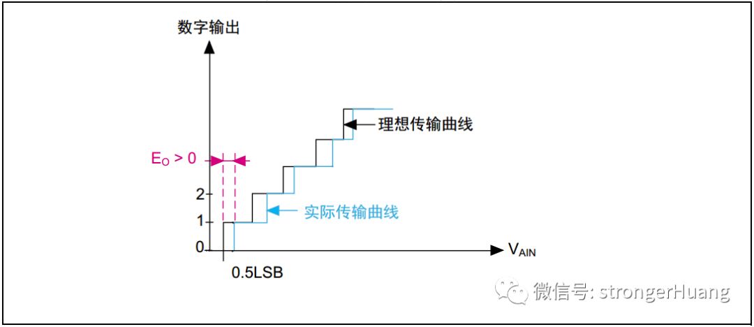
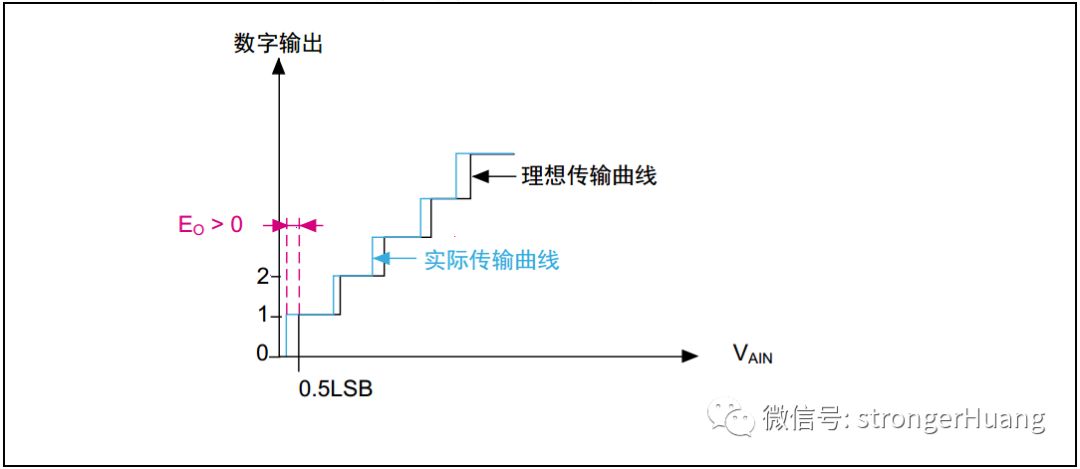
Offset error is the deviation between the first actual conversion and the first ideal conversion. The first conversion occurs when the digital ADC output changes from 0 to 1. Ideally, when the analog input is between 0.5 LSB and 1.5 LSB, the digital output should be 1.
Still, ideally, the first conversion occurs at 0.5 LSB. Let EO represent the offset error. Offset error can be easily calibrated by applying firmware.
Representation of Positive Offset Error:
Representation of Negative Offset Error:
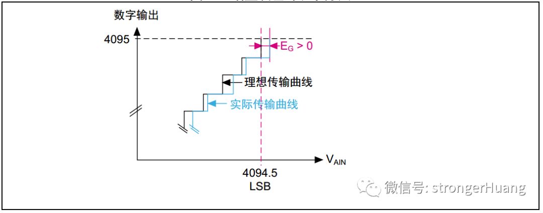
Gain error is the deviation between the last actual conversion and the last ideal conversion. Gain error is represented by EG.
Representation of Positive Gain Error:
Representation of Negative Gain Error:
(3) Differential Linear Error
Differential linear error (DLE) is the maximum deviation between the actual step and the ideal step. The “ideal situation” here does not refer to the ideal transfer curve but to the ADC resolution.
Ideally, a change in analog input voltage of 1 LSB should cause a change in digital code. If more than 1 LSB of analog input voltage is required to cause a change in digital code, differential linear error will be observed. Thus, DLE corresponds to the maximum additional voltage required to change from one digital code to the next.
(4) Integral Linear Error
Integral linear error is the maximum deviation between any actual conversion and the endpoint-related line, represented by EL.
The endpoint-related line can be defined as the line connecting the first actual conversion and the last actual conversion on the A/D transfer curve. EL refers to the deviation from this line for each conversion. Thus, the endpoint-related line corresponds to the actual transfer curve and is unrelated to the ideal transfer curve.
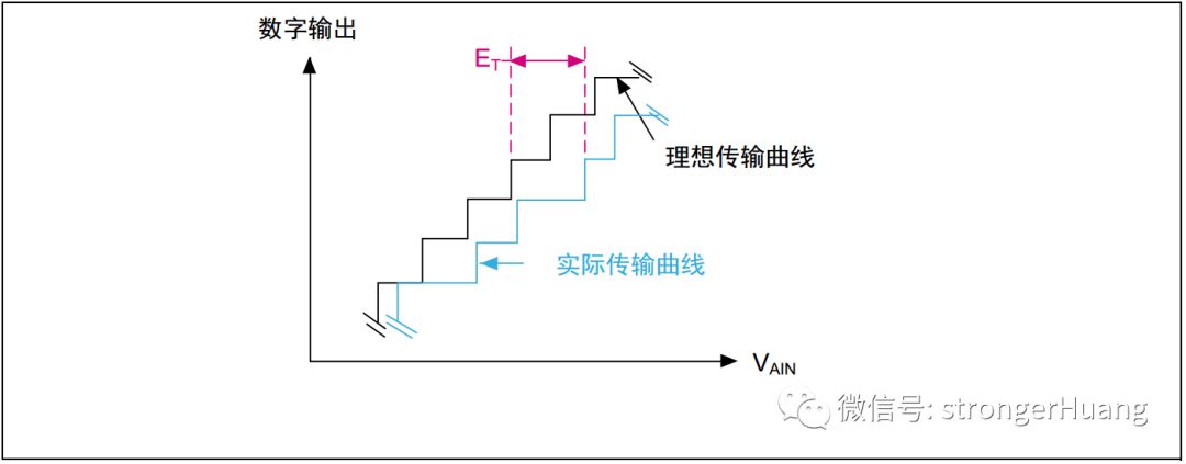
(5) Total Unadjusted Error
Total unadjusted error (TUE) is the maximum deviation between the actual and ideal transfer curves. This parameter specifies the total error that may occur and causes the maximum deviation between the ideal expected value of any input voltage and the actual value obtained from the ADC.
2. Errors caused by the ADC environment
(1) Reference Voltage Noise
Since the ADC output is the ratio of the analog signal voltage to the reference voltage, any noise on the analog reference will cause a change in the digital value after conversion. In some packages, the VDDA analog power supply is used as the reference voltage (VREF+), so the quality of the VDDA power supply will affect the ADC error.
(2) Reference Voltage/Power Regulation
Power regulation is crucial for ADC accuracy since the conversion result is the ratio of the analog input voltage to the VREF+ value.
When connected to VDDA or VREF+, if the load on these inputs and their output impedance cause the power output to drop, this will introduce errors in the conversion results.
(3) External Reference Voltage Parameters
When using an external reference voltage source (on the VREF+ pin), this external reference source has some important parameters. Three reference voltage specifications must be considered: temperature drift, voltage noise, and long-term stability.
(4) Analog Input Signal Noise
During the sampling period, small and high-frequency signal changes can lead to significant conversion errors. This noise is generated by electrical devices (such as motors, engine ignition, power lines). It adds unwanted signals, thus affecting the source signal (like sensors). This leads to inaccurate ADC conversion results.
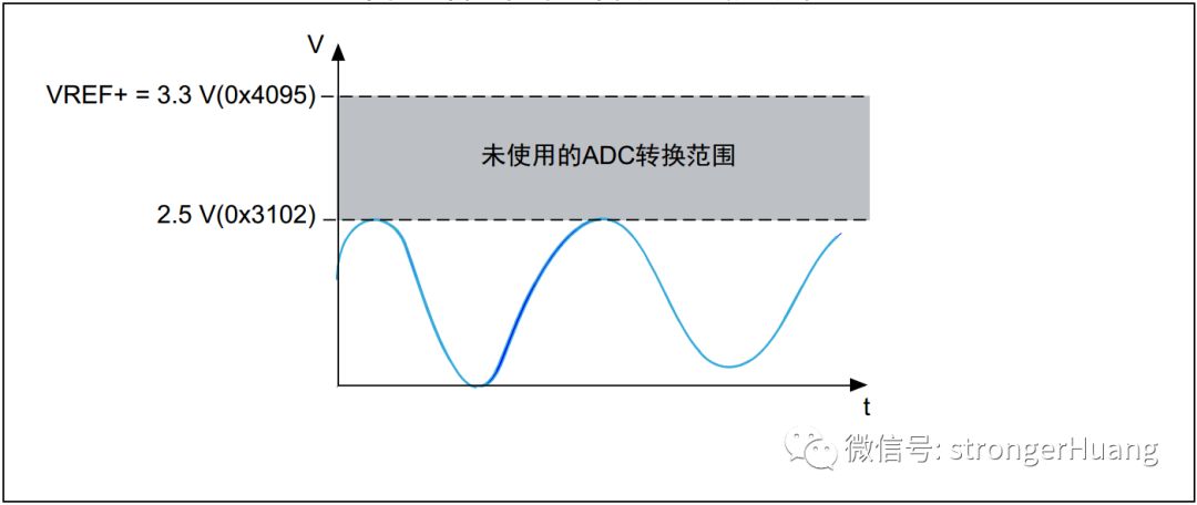
(5) Poor Matching of ADC Dynamic Range to Maximum Input Signal Amplitude
To achieve the highest ADC conversion accuracy, the ADC dynamic range must match the maximum amplitude of the signal to be converted.
Assuming the signal to be converted varies between 0 V and 2.5 V, and VREF+ equals 3.3 V. As shown below, part of the unused ADC conversion range will also reduce the accuracy of the converted signal.
How to Improve the Accuracy of ADC Data Collection
This issue has been previously addressed, but it has not been highlighted separately, so here is a summary.
1. Reduce the Impact of ADC-Related Errors
The above described “errors caused by the ADC itself,” using the STM32 ADC self-calibration function or through microcontroller firmware can easily compensate for offset and gain errors.
Previously shared code mentioned, for example, through software correction:
ADC_StartCalibration(ADC1);
2. Minimize Environmental Errors
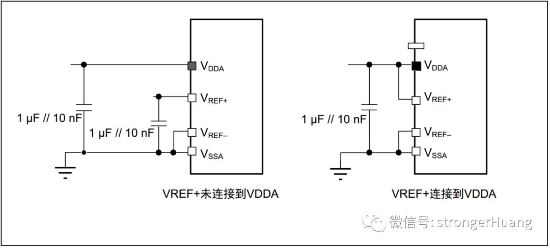
(1) Minimize Reference Voltage/Power Noise
This means connecting external decoupling capacitors to the VREF and VDDA pins.
(2) Eliminate Analog Input Signal Noise
This can be done by adding an external RC filter to eliminate high frequencies.
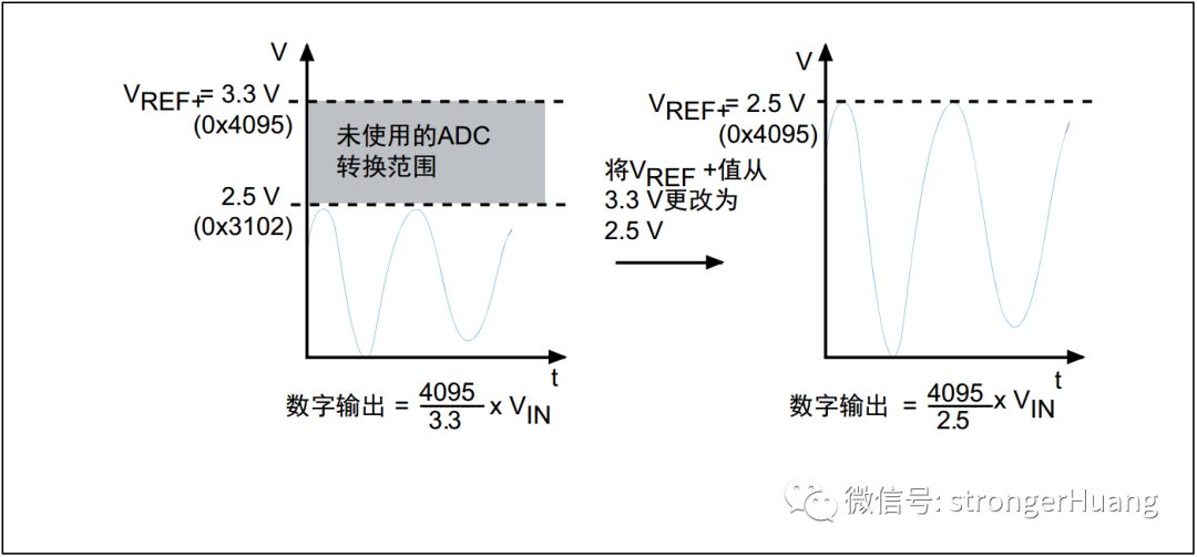
(3) Match ADC Dynamic Range to Maximum Signal Amplitude
This means matching the reference voltage range to the sampling voltage (of course, this requires a chip with reference voltage pins).
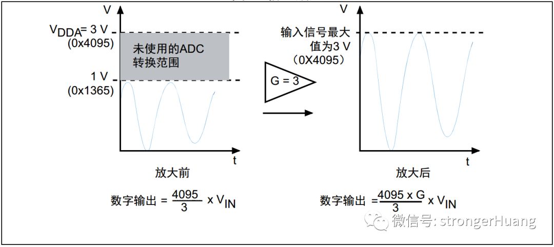
At the same time, amplifiers can be used to adjust the input signal range for the ADC:
(4) Temperature Impact Compensation
The first method is to fully describe the characteristics of offset and gain drift and provide a lookup table in memory to correct measurement values based on temperature changes. This calibration method requires additional cost and time.
The second method involves using an internal temperature sensor and ADC watchdog to recalibrate the ADC when temperature changes reach a given value.
3. Software Methods to Improve Accuracy
(2) Digital Filtering (Suppressing 50/60 Hz Noise in DC Values)
(3) Fast Fourier Transform (FFT) for AC Measurement
(4) ADC Calibration: Offset, Gain, Bit Weight Calibration
(5) Minimize Internal Noise Generated by CPU
The application design must ensure:
Well, this concludes the article. I hope it can be helpful to everyone.
Copyright belongs to the original author. If there is any infringement, please contact for deletion..
Share an embedded data visualization tool
The Eight Realms of Programmers, Which Layer Are You In?
I Used This Technology to Eliminate Thousands of Lines of If Else!
→ Follow for More Updates ←