From wafer cleaning to etching and packaging, specialty gases with a purity of 99.999% permeate 400 processes, serving as the “invisible framework” participating in chemical reactions and being a decisive variable for chip performance and yield—scientific gas selection and safe gas usage are uncompromising precision arts in semiconductor manufacturing..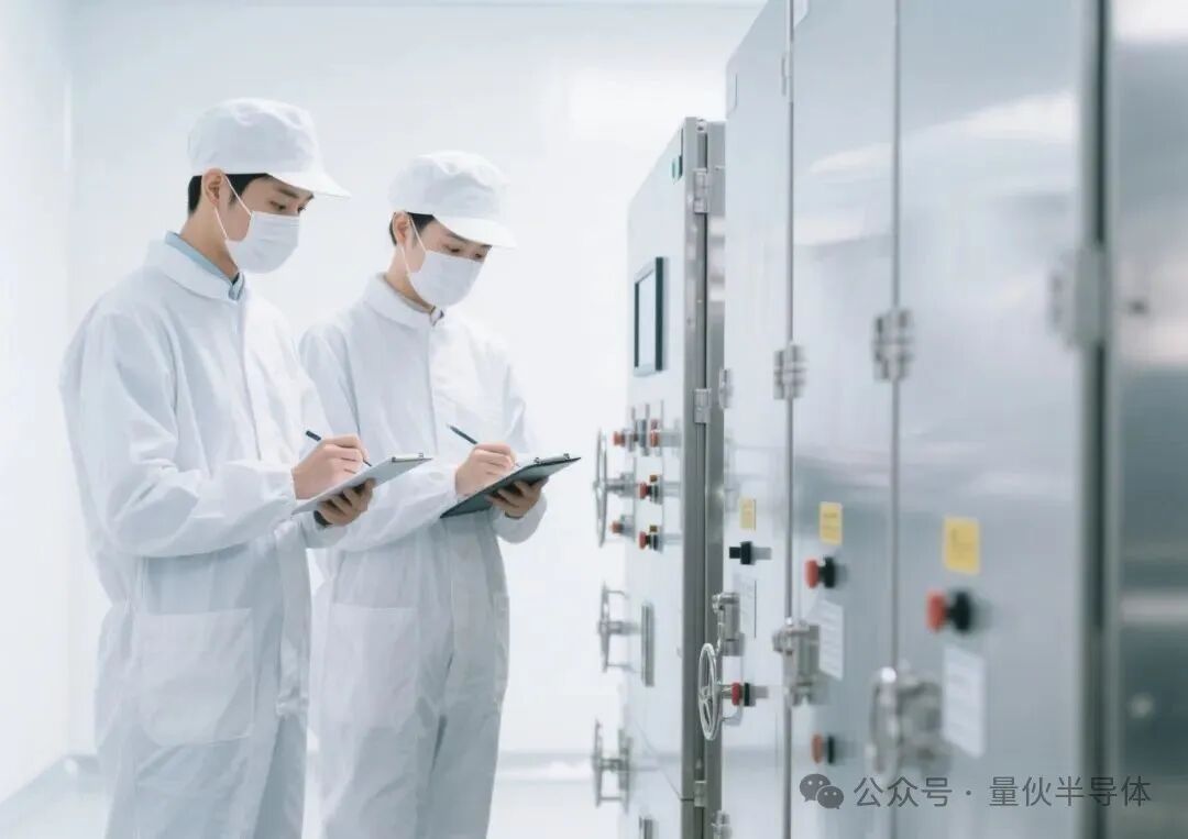
Semiconductor wafer manufacturing is an extremely complex micro-nano process involving over 400 high-precision steps, which impose nearly stringent requirements on material selection, environmental control, and chemical reaction conditions. Among these, specialty gases, as one of the core process materials, run through the entire manufacturing process, from wafer cleaning, doping, deposition, etching, to interconnection and packaging, where the purity, reactivity, and stability of the gases directly determine the chip’s performance, yield, and consistency.

● From Wafer to Chip: The Role of Gases in Key Processes:
In the front-end processes of wafer fabrication, gases are not just auxiliary materials but core participants directly involved in reactions.
● During the wafer cleaning stage, high-purity nitrogen is used for drying to avoid surface oxidation, combined with hydrogen, ammonia, or ozone to effectively remove organic substances, particles, and metal ions.The combination of ammonia and hydrogen peroxide (SC1 process) is a widely used deionized cleaning method in the industry. This stage requires extremely high gas purity, typically needing to reach above 99.999% (5N) to avoid secondary contamination.
● In the doping step, introducing specific impurity atoms (such as phosphorus, boron, arsenic) is crucial to alter the electrical conductivity of silicon crystals.Common doping gases include phosphine (PH₃), diborane (B₂H₆), and arsine (AsH₃), which are usually used with hydrogen as a carrier gas. These gases are often highly toxic and corrosive, requiring dilution and strict leak detection and exhaust treatment systems.
● In the thin film deposition stage, gases such as silane (SiH₄), dichlorosilane (SiH₂Cl₂), ammonia (NH₃), and nitrous oxide (N₂O) are used in CVD or ALD processes to build various dielectric layers, conductive layers, and protective films. The deposition reactions highly depend on the stability of gas flow and reactivity, directly affecting the thickness, uniformity, and interface quality of the film layers.
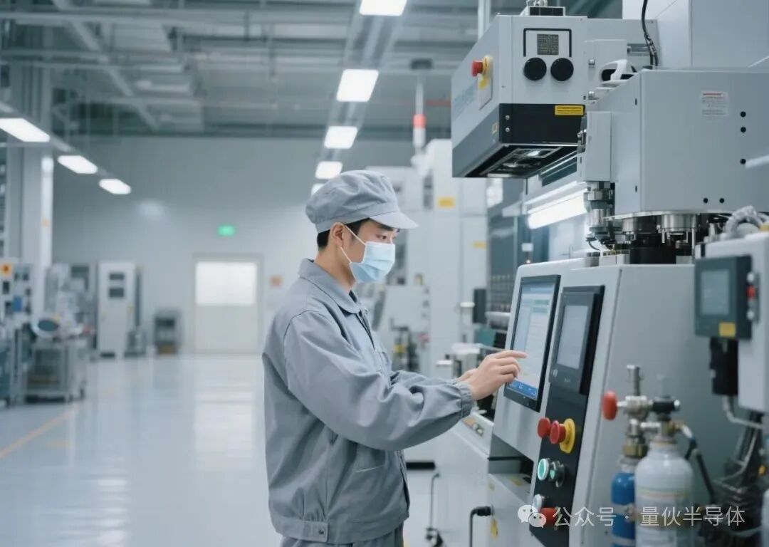
● After lithography and development processes, to remove residual photoresist and organic impurities, a combination of ozone, oxygen, and nitrogen is typically used for plasma-assisted cleaning. These gases ensure the clarity of pattern transfer and lay the foundation for subsequent etching.
● In the etching stage (especially dry etching), gases such as carbon tetrafluoride (CF₄), sulfur hexafluoride (SF₆), chlorine (Cl₂), nitrogen trifluoride (NF₃), and fluorine (F₂) are used as etching gases to form plasma for precise removal of selected areas. These gases need to have high reactivity, good directionality, and volatility of reaction by-products to meet etching precision at extremely small dimensions.
● During the metallization and interconnection process, hydrogen, argon, and nitrogen are used for pretreatment or protective atmospheres; certain metals like copper require CVD gases containing organometallic precursors for fine structural detail construction.
● Finally, in the chip packaging and testing stage, nitrogen is used for laser welding protection and chip drying, helium for precision gas-tightness testing, and hydrogen/nitrogen mixtures are applied in processes like atmosphere annealing to ensure device stability.
Throughout the entire process, gases are always involved, reacting, protecting, and controlling, serving as the true “invisible framework” in chip manufacturing.

● How to Scientifically Select Gases?▼
The correct gas selection should be centered around the process objectives. Each process step corresponds to different gas types, concentrations, purity levels, reactivity, and safety requirements.
For example
● Doping requires active molecules that can provide electrons or holes, with phosphine and diborane being the preferred choices;
● Etching processes require halogen gases with good plasma stability and etching selectivity;
● Cleaning and protection processes place more emphasis on the inertness, oxidation capability, or drying performance of gases;
Among all selection factors, purity is always one of the most important parameters. In semiconductor manufacturing, 5N (99.999%) is the basic threshold, while high-end processes may even require 6N or 7N. Even a millionth of an impurity can cause defects, disconnections, or performance drift in sub-micron device structures.
Additionally, it is necessary to comprehensively consider the toxicity, corrosiveness, environmental impact, and supporting treatment capabilities of gases:
For example
● Nitrogen trifluoride, while having high etching and cleaning efficiency, possesses a high greenhouse effect and toxicity, necessitating the configuration of a plasma exhaust decomposition system;
● For highly toxic gases like phosphine and arsine, gas detection devices, dilution protection, and automatic emergency shut-off systems must be equipped;
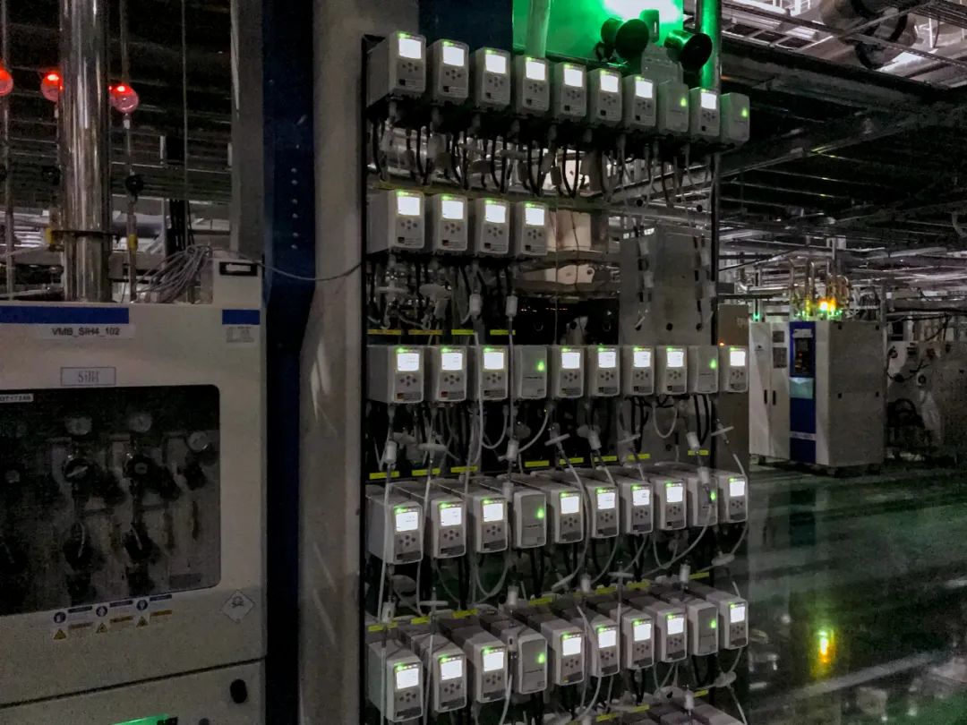
In some processes, balancing choices based on cost, gas supply stability, and system compatibility is also necessary. For example, whether to use diluted gases instead of pure gases, or whether to adopt mixed gas ratios to optimize process windows, are decisions that weigh both technology and cost.

● How to Standardize and Safely Use Gases?
Choosing the right gas is just the first step; standardized and safe usage is the key to ensuring process success..
First, a professional gas supply system must be used
including gas cabinets with automatic switching and pressure regulation, high-purity electropolished stainless steel pipelines, VCR sealing interfaces, and real-time gas monitoring and alarm systems. All components must have corrosion resistance, easy cleaning, and leak-proof characteristics to ensure no cross-contamination or gas residue occurs during continuous operation.
Secondly, all gas usage must be equipped with
a complete status monitoring system
including information on cylinder pressure, gas remaining, flow rate, purity, etc. Critical gases should be equipped with gas leak detectors, and important production lines should also be paired with exhaust purification equipment to avoid the discharge of toxic/harmful gases.
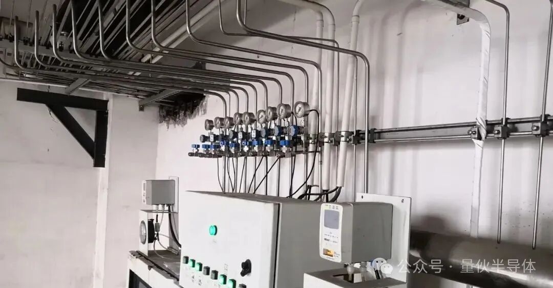
Storage and Transportation Management
In storage and transportation management, gas cylinders must be transported according to hazardous materials requirements, classified and stored in a dedicated area that is ventilated, dry, and away from heat sources, and equipped with fixed devices to prevent tipping. Pressure regulators, gas pipes, and other connectors should not be mixed and should be managed according to gas type with dedicated numbering.
Standard gases and multi-component mixed gases also require special attention to shelf life and stability of composition; they should be thoroughly shaken before use to avoid stratification. Operators must undergo professional training to master MSDS requirements and emergency response procedures.

In the extremely precise “nano road” of semiconductor manufacturing, gases are not merely auxiliary materials, but core variables deeply involved in reactions, controlling processes, and ensuring yield. From every reaction on the wafer surface to every contour of the etched pattern, and to the doping control of every layer of impurities in microstructures, these invisible chemical roles are indispensable.
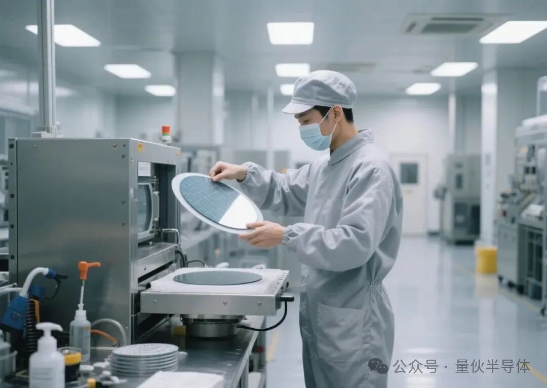
For manufacturing enterprises, scientifically selecting gases and standardized gas usage not only reflects technical capabilities but also fundamentally guarantees product quality, production efficiency, and operational safety. For practitioners, understanding the performance of gases and process compatibility is a key step from execution to optimization.
Safety in production is a major issue related to the safety of people’s lives and property, and a mark of coordinated economic and social development. In the production process, by installing gas detection and alarm devices, continuously monitoring the concentration of toxic and harmful gas leaks, risks can be controlled at the source.


Hydrogen Power in Chip Manufacturing: How to “Turn Stone into Gold” in the Semiconductor Industry
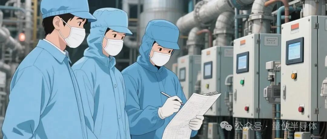
Safety Production Month is approaching, and frontline personnel in the semiconductor industry must know the “Safety Survival Guide”
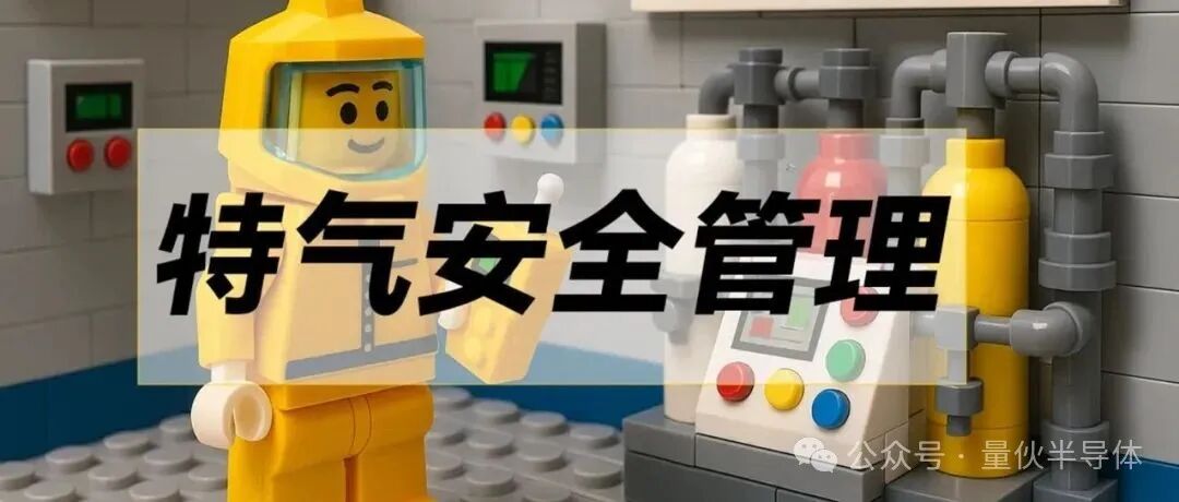
Semiconductor Factory Manual | Suggestions for Specialty Gas Safety Management
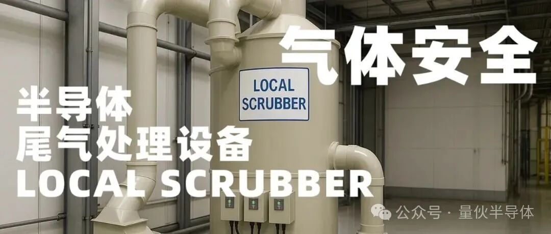
Gas Safety in Local Scrubber for Semiconductor Process Exhaust Treatment Equipment
Rigor is a belief, focus is an attitude
Click “View”, “Share”, “Like” to encouragecontinued creation
Your support isSemi Safe’s continuous update motivation Note: Some images and texts in this article are sourced from the internet for learning and communication purposes. If there is any infringement, please contact for removal.