In the world of chip manufacturing, the race at the nanoscale has never ceased.
As we transition from 7nm to 5nm, 3nm, and even more advanced processes, an unexpected challenge has emerged: the power delivery network is starting to occupy the front space of the chip.
It’s like a bustling city where utility poles and cables gradually fill the streets, causing severe traffic congestion.
Chip designers face a similar dilemma until they conceived a revolutionary solution: moving the power system from the “ceiling” of the chip to the “floor”.
This is the core idea of Backside Power Delivery Network (BSPDN) technology—flipping the power delivery network from the front of the wafer to the back.
A revolution in power delivery within the semiconductor industry has begun.
01
—
Power Delivery Dilemma: The “Congestion Crisis” on the Chip Front
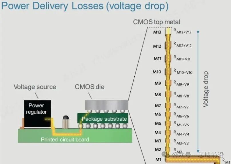
As transistor sizes continue to shrink and densities increase, the number of stacked layers also rises, making it necessary to power transistors and transmit data signals through 10-20 layers of stacks, significantly increasing the complexity of line design.
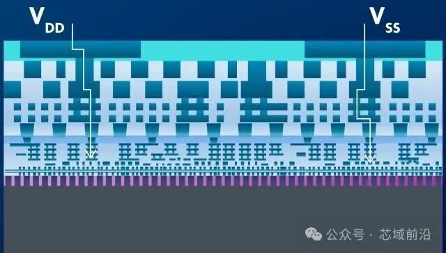
In traditional chips, power lines and signal transmission lines coexist on the front of the chip.
This design leads to the power network competing for limited spatial resources with the signal network, exacerbating interference issues.
Power lines occupy about 20% of the front space of the chip.
This results in more severe interference between signal lines and power lines, also limiting further increases in transistor density.
Worse still, when current needs to pass through complex metal layers to reach the transistors below, the path length increases, resistance rises, leading to reduced power delivery efficiency, increased power consumption, and voltage drop issues.
Chip designers face a seemingly unsolvable dilemma.
02
—
Technological Disruption: The Power Delivery Revolution from “Ceiling” to “Floor”
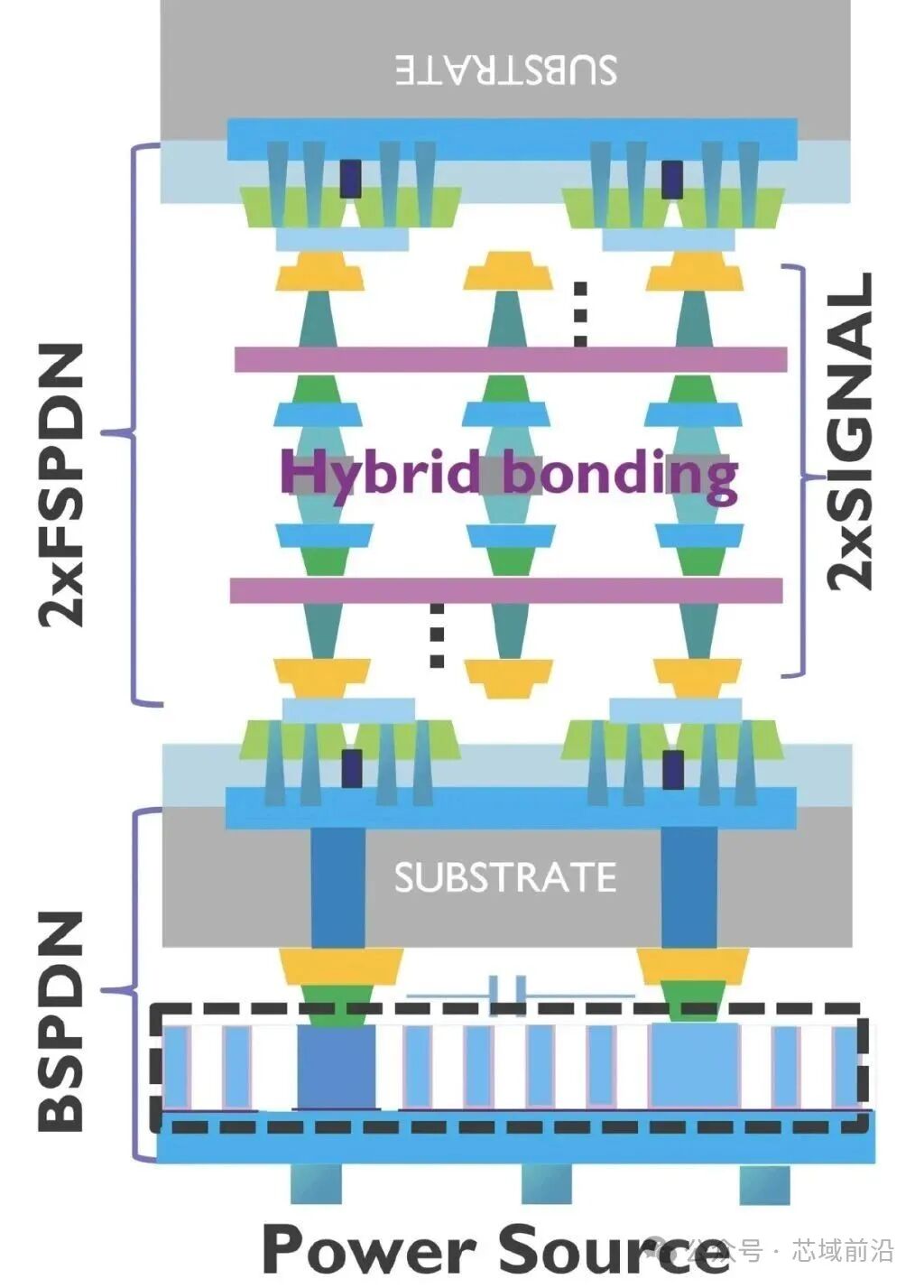
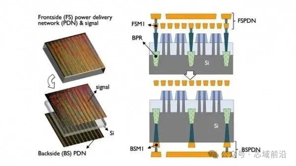
The basic concept of Backside Power Delivery Network (BSPDN) technology is simple yet highly disruptive: migrating the entire power delivery network from the front of the wafer to the back.
Power is transmitted directly from the back to the front through Through-Silicon Vias (TSVs), eliminating the need for electrons to traverse the increasingly complex Back End of Line (BEOL) stack on the chip’s front.
This method achieves a complete decoupling of power transmission and signal networks.
IMEC (Interuniversity Microelectronics Centre) first proposed the concept of backside power delivery in 2019, and subsequently, major chip manufacturers worldwide have followed suit to develop their own solutions.
-
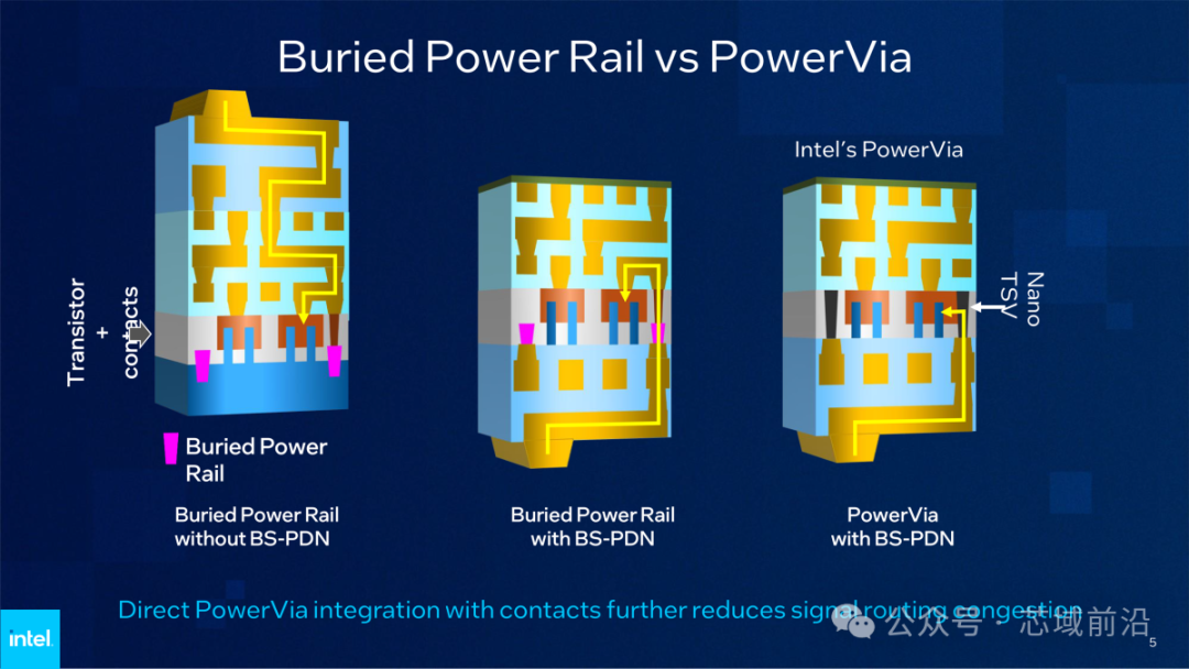
Intel calls it “PowerVia” and plans to adopt it for the first time at the Intel 20A node;
-
TSMC has introduced the “Super PowerRail” solution;
-
Samsung is also actively incorporating BSPDN technology into its 2nm process development roadmap.
03
—
Technological Competition: The BSPDN Strategic Layout of the Three Giants
The three giants of the semiconductor industry—TSMC, Samsung, and Intel—are heavily investing in BSPDN technology, but each has chosen different technical paths and implementation timelines.
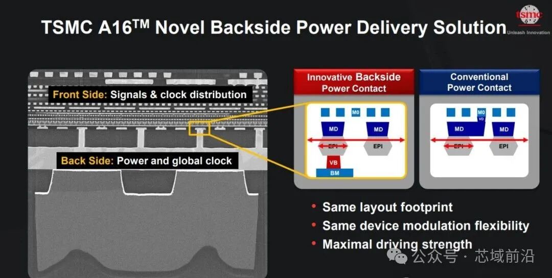
TSMC has opted for the most direct and efficient yet complex and costly production solution.
In its A16 node process technology, the power transmission lines are directly connected to the source and drain.
TSMC claims that at the same operating voltage, the A16 node using Super PowerRail is 8-10% faster than N2P;
at the same operational speed, power consumption is reduced by 15-20%, and chip density is increased by up to 1.10 times.
Samsung plans to introduce BSPDN technology into its 2nm process by 2025.
Preliminary test results show that this technology can reduce chip area by 10% and 19% respectively.
Lee Sungjae, Vice President of Samsung’s Foundry Process Design Kit Development Team, revealed that compared to traditional front-end power delivery networks, BSPDN can improve chip performance and power by 8% and 15%, respectively.
Intel is the first to adopt PowerVia backside power delivery technology at the Intel 20A node, expected to be production-ready in the first half of 2024.
The Intel team created the “Blue Sky Creek” test chip to demonstrate this method, allowing power lines and interconnect lines to be separated and made thicker, while improving power delivery and signal transmission.
04
—
Manufacturing Challenges: The Art of Balancing Precision and Cost
While BSPDN technology brings significant advantages, its manufacturing process is exceptionally complex, involving multiple high-difficulty and closely interconnected process technologies.
The challenge of backside power delivery lies in the need to grind the back of the wafer to a thickness that nearly touches the transistors.
However, this significantly reduces the rigidity of the wafer, necessitating the bonding of a carrier wafer to the front of the wafer to support the backside manufacturing process.
In the nTSV (nano-silicon via) process, to ensure uniform copper metal coating in the nanoscale vias, more equipment is needed for assistance in detection.
The manufacturing process of BSPDN mainly includes several key steps:
First, a layer of silicon germanium (SiGe) is grown on a standard silicon wafer as an etch stop layer, followed by a thin silicon cap layer, marking the beginning of the manufacturing of components and buried power tracks.
Next, the wafer bonding stage occurs, where the silicon wafer is aligned and bonded to the carrier wafer, followed by annealing to strengthen the bond between the two.
Then, through chemical mechanical polishing (CMP) technology combined with dry and wet etching, thinning is performed, gradually removing the upper silicon material until the SiGe layer is exposed.
After removing the SiGe layer, the back of the chip is prepared, followed by nano-scale silicon via (nTSV) processing.
Nano-scale silicon vias require first depositing a passivation layer on the back of the wafer, then performing multiple steps such as via drilling and filling, followed by atomic layer deposition (ALD) technology to form an insulating layer on the via walls, and finally filling with tungsten (W) as a conductor to complete the electrical connection.
05
—
Performance Leap: Significant Advantages Brought by BSPDN
After adopting BSPDN technology, chip performance and energy efficiency have significantly improved.
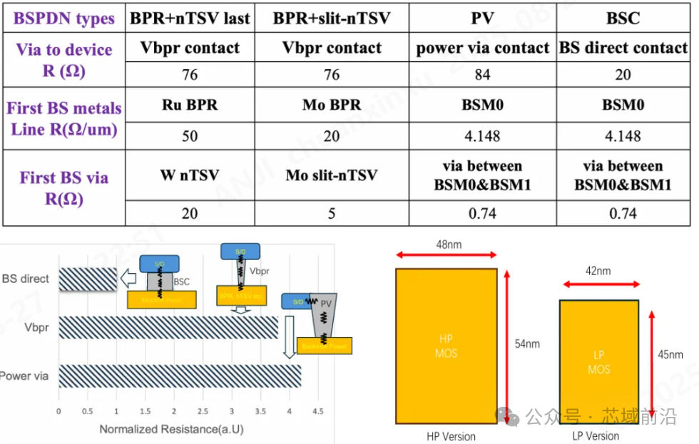
According to research evaluations by IMEC and Arm, compared to front-end PDN, BSPDN achieves a 6% frequency and 16% area improvement, with no drawbacks in energy consumption.
Samsung’s research shows that BSPDN technology can reduce chip area by 14.8% and wiring length by 9.2%.
This helps to lower resistance, allowing more current to flow, thereby reducing power consumption and improving power transmission conditions.
TSMC expects that its N2P process’s backside PDN will improve performance by 10-12% by reducing IR Drop and enhancing signals, while reducing logic area by 10-15%.
These advantages will be even more pronounced in high-performance CPUs and GPUs with dense power delivery networks.
BSPDN technology can also address the increasingly severe power delivery issues in transistor scaling.
As copper wires shrink, resistance begins to rise exponentially.
By utilizing the backside of the bottom wafer for power transmission and signal routing, additional performance gains can be achieved.
06
—
Future Prospects: Market Opportunities and Development Trends of BSPDN Technology
According to statistics and forecasts from market research firm QYResearch, the global BSPDN technology market sales are expected to reach $0.13 billion in 2024, and are projected to reach $0.44 billion by 2031, with a compound annual growth rate (CAGR) of 13.7% (2025-2031).
The Chinese market has changed rapidly in recent years, with the market size expected to account for a certain proportion of the global market in 2024, and further growth anticipated by 2031.
BSPDN technology is primarily applied in advanced processes such as 3nm and 2nm chips.
In the future, BSPDN technology will continue to evolve.
IMEC and its industry partners are exploring what other functions can also be migrated to the back, such as global interconnects and clock signal distribution.
This development brings new challenges and opportunities for “functional backside” (or backside 2.0). The backside power delivery network technology has quietly developed into a technical concept in the entire chip manufacturing industry over the past few years.
In the future, all leading chip foundries will turn to this technology. This power delivery revolution will bring new momentum to the semiconductor industry.
BSPDN technology is reshaping the landscape of chip manufacturing.
The technological race among TSMC, Samsung, and Intel is accelerating the commercialization of this technology.
It is expected that by 2031, the global BSPDN technology market size will reach $44 million, and this figure may just be the beginning of a larger explosion.
Chip power delivery has flipped from the “ceiling” to the “floor”, and this revolution is redefining the future of the semiconductor industry.
 Original Statement: This article is a compilation of publicly available information,reproduction requires authorization.If you like it, please give it a“Like”.