Table of Contents
1 Introduction
2 The First Wave (2008-2013)
2.1 Starting Point2008
2.1.1 Calxeda 2011
2.2 Computex2012
2.3 MarvellArmada XP 2013
2.4 CalxedaBankruptcy 2013
3 The Second Wave Armv8.0 (2011-2018)
3.1 AppliedMicro – X-gene (2011)
3.1.1 eMAG-X-Gene32018
3.2 AMD’sA1100 (2012)
3.3 CaviumThunderX 2014
3.4 BroadcomVulcan ThunderX2
3.5 Qualcomm2017
3.6 Samsung(2012-2014)
3.7 NvidiaProject Denver 2011-2014
3.8 Balkal
3.9 Phytium
3.10 HiSilicon1616
3.11 Socionext
3.12 Personal Comments
4 The Third Wave Neoverse
4.1 HuaweiKunpeng 920
4.2 AWSGraviton2
4.3 AmpereQuickSilver 2019
4.4 MarvellThunderX3
4.5 FujistuA64FX 2016
4.6 Other New Entrants
5 Conclusion
6 References
1 Introduction
This article is prepared for internal technical sharing within the company. Of course, if I dare to talk about it from 2008, I would have been killed long ago. Also, the NDA content is certainly omitted.
If I were to summarize my journey in the Arm server industry over the years in one sentence, it would be “Through hardships and difficulties, to open up the mountain forest.”
Disclaimer:Personal views, do not represent any company. The data cited in the article comes from public news and conferences.
To help everyone know who I am, I give myself a label: a person who has been responsible for everything from CPU PPT to cloud computing.
2 The First Wave (2008-2013)
The first wave of Arm servers started with a company called Calexda and ended with it. Although I think the official announcement of the Armv8 architecture in 2011 signifies the end of 32-bit servers, the fluctuations of the first wave were not just about 32-bit and 64-bit, but also a term called Microserver, which was a common exploration in the industry, including the x86 camp. Technically and commercially viable products did not succeed in the market.
One observation I have made is that the server market is a stable and conservative market, compared to the active terminal market.
2.1 Starting Point 2008
In 2008, the internal plan for Arm servers began to take shape. When the heart moves, action is taken. Arm invested in a startup called Smooth Stone, which later changed its name to Calexeda. The total investment amount in the first round was $48M.
The initial goal of Calexeda was to reduce energy consumption in data centers and increase computing density in the same space. Remember these two goals; at this moment, our original intention remains unchanged.
At that time, the market was still dominated by Cortex-A8 products, while the first multi-core product based onCortex-A9 would not be released until 3 years later. (I miss the slow era when it took 2 or 3 years to release a product).
At that time, Intel’s Xeon was still 4 cores, of course the main frequency had already reached 3.xGhz, while AMD’s 45nm Opteron CPU had just been released.
That year, IBM announced the Power product line, starting with a staggering 64 cores.
Apple released the iPhone 3G, which was the iPhone2. (Yes, it was still the 3G era).
TSMC’s mainstream process was 40nm, with an annual revenue of $10B.
I was still working at a company called EZchip doing NP3, where NP does not mean Neural Processor but Network Processor. It was a prosperous era for network processors, and I could list a long string of names, but unfortunately, most of them are now forgotten. Just a little low-key bragging: my strongest part was TM-Traffic Manager and not just the processor part; this is also the most prominent feature of this Israeli company with over 100 employees (annual revenue of about $60M). A lot of text is omitted here; if I were to talk in detail, I could give a week-long training, the kind that charges in USD.
2.1.1 Calxeda 2011
In 2010, Smooth Stone officially changed its name to Calexeda and moved its headquarters to Austin.
In 2011, Calexeda released its chip based on A9 called EnergyCore ECX-1000.
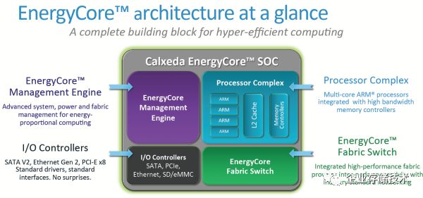 Figure 2.1CalexedaEnergyCore Architecture
This is actually a design worth looking into, a 4-core cortex-a9 processor module, quite standard. The I/O controllers part is also a regular interface (regular interfaces are not easy; the core of a good product is to achieve industry-leading in regular parts). However, the management engine (management engine) and the switching engine (Fabric Switch) are very innovative technologies.
EnergyCore Fabric is an integratedL2 switch supporting mesh, butterfly tree, 2D Torus topology, the bandwidth between virtual ports can be allocated according to1 Gb/sec, 2.5Gb/sec, 5 Gb/sec, and 10 Gb/sec specifications.Through it, server nodes can autonomously form networks without going through the on top switch, thus Calexeda can have 4 chips on one board, which means 16 cores. Therefore, it can have up to 480 cores in a server system.
This design concept is reasonable; if you design a very low-cost server chip, but the supporting network is still expensive, high-density design will only increase costs. This fabric can connect 1024 system boards, meaning 4096 chips using 10G network interfaces into a system.
EnergyCore ManagementEngine is an integratedBMC that supports IMP2.0 and DCMI, and also supports remote debugging SoL protocol. The strongest feature of the management engine is power management; the power consumption of Calexeda’s server chip can dynamically adjust from 4w to 1w.
The manufacturing cost of each node is about $28.
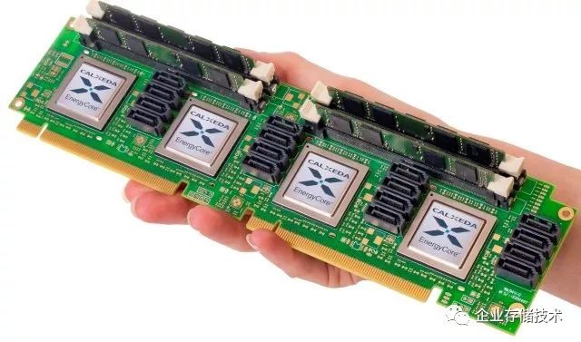
Figure 2.2 4 nodes ofCalexeda system board
In 2011, I joined the network marketing department of Arm. At that time, I was focused on the design stage of the LSI Axxia AXM5500 16-core ARMCortex-A15, Freescale’s QorIQ Layerscape series, TI’s KeyStone, and HiSilicon’s hixxxx series. That was indeed an explosive era for Arm in the network market. However, soon after, a year later, I followed my then-boss, a senior beauty of Indian descent with a movie star aura, and transitioned from the network market to the server market, dedicating myself to the server market and ecosystem construction ever since.
2.2 Computex 2012
In 2012, Ian Ferguson gave a public speech at Computex in Taipei, which was about Arm’s first introduction to the public regarding its efforts in the server domain. Standing with him was Ubuntu’s Mark (the software ecosystem is a big topic; this article mainly focuses on chips, and system hardware design and software topics will be discussed in another article). He quoted Facebook’s Frank’s perspective on performance per watt per dollar.
When mentioning Arm servers, Ian Ferguson must be mentioned (he taught me a fundamental sentence for marketing work: “Are you going to report news, or make news?” Now I also like to say with my friends, come, let’s do something together.) As he stated at the conference, from the first day Arm considered the server market, the entire industry was filled with skepticism. Not only doubting whether it could succeed, but fundamentally doubting the motivation.
These questions, I am not in a hurry to answer; if you have the patience to read to the end, everything will have its own answers.
2.3 Marvell Armada XP 2013
In the first wave of server trends, Marvell Armada XP quad-core series also deserves mention. Moreover, the core here is neither A9 nor A15, but Marvell’s custom Core.
It was because of Armada that I became proficient in what architecture licensing means.
Figure 2.3 MarvellArmada XP
This highly integrated, low-power SoC is very suitable for storage applications. Dell used it as the core for its Copper arm server system. Baidu also used it at one point. This was the first case of Arm servers in internet companies.
2.4 Calxeda Bankruptcy 2013
If Calxeda could have raised its third round of investment, then according to the roadmap below, there would be an A15 chip ready for mass production and 2 Armv8 chips in the plan. However, unfortunately, the fundraising efforts were unsuccessful. Calxeda was founded in 2008 and went bankrupt in 2013, with a total investment of $103M ($48m in 2010 & $55m in 2012), with a total of 130 employees.
In its closure email, it stated that due to the emergence of Arm servers, “the industry will be transformed forever.” Looking back now, it is indeed the case.
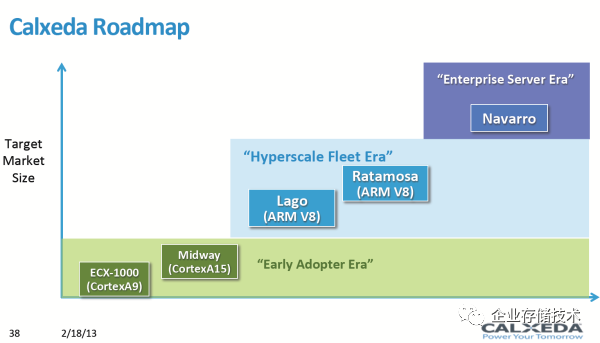
Figure 2.4 Calxeda Roadmap
Insight 64’s analysts said they spent too much money on 32bit Arm servers. Indeed, in 2011, Arm announced the 64bit Armv8, and Applied Micro announced the X-gene plan. In fact, the second wave of Armv8 server trends had already begun.
Calxeda’s bankruptcy marked the end of the first wave.
3 The Second Wave Armv8.0 (2011-2018)
Although I have given this piece a literary title, I intend to write it as a technical analysis article, focusing on the characteristics and evolution of Arm server chips, rather than explaining why this company succeeded or that company failed. In fact, product analysis is relatively straightforward, while the success or failure of a company is greatly influenced by random factors.
The three keywords of the second wave are self-researched cores (custom core), mainstream performance, and standard design. In the early years of Arm servers, chip design companies came from various fields, each bringing their understanding of server CPU chips and delivering their products. I focus on APM’s X-gene, Cavium’s ThunderX, and Qualcomm’s Centriq 2400. I also strive to provide clues about all other chips for those interested to explore further.
I created an Excel sheet to compare all server SoCs, including company size, investment, and human resources. Let’s meet offline for discussions.
Let me also mention that in this historical period, self-researched cores accounted for the majority, and the debate about architecture and ISA has been ongoing. I do not wish to elaborate on this as it may deviate from the topic. I learned a term from a big player in private cloud, “cumulative advantage.” In making CPUs, designing ISAs, and making chips, it is indeed a slow accumulation of advantages. Over the years, I have gone to headquarters with customer demands, cases, and test data, confidently asking architects or product managers to change designs and add instructions (yes, I was also involved in this), and the results? I cannot say I have never succeeded, but my architects and product managers are tough characters, and they rarely lose in data and application case competitions.
Additionally, Hock Tang must be mentioned; this man is simply a thorn in the path of Arm servers and my career, a man who has achieved double kills. He first acquired Broadcom, sold off the server chip project, and then proposed acquiring Qualcomm. The management of Qualcomm, in self-preservation, proposed to cut $1B in expenses each year, thereby self-terminating all long-term investment projects, and the well-functioning server projects were thus collateral damage.
3.1 AppliedMicro – X-gene (2011)
In October 2011, when Arm first announced the ARMv8 architecture, Applied Micro announced their self-architecture x-gene plan (big news is often released together with key customers).
If you read news back then, you would have noticed the concept of SoC. Now, there is no need to explain SoC. At that time, it was still important to emphasize that SoC equals chip + chipset integrated design.
The first generation of X-gene has 8 self-researched cores -Storm, two cores sharing 256KB of L2 cache, which differs from Arm’s 4 cores in a cluster. The Opteron A1100 processor from AMD that I will discuss next chapter also did not use 4 Cortex-A57 in one cluster, but rather a design of 2 A57 and 4 clusters. AMD’s A1100’s two A57 share 1MB of L2 cache, which is four times larger than X-gene’s self-researched core Storm, which is 4 issue designs, while A57 is still at the sweet spot of 3 issue efficiency ratio.
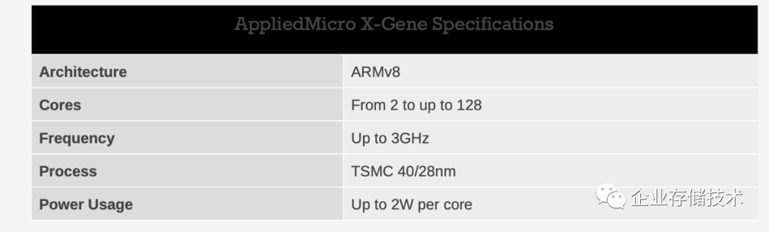
Figure 3.1 APM’s X-Gene specifications
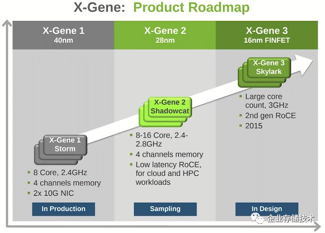
Figure 3.2 APM’s X-Gene product roadmap
Now, even mobile CPUs are heading towards 6 issue, from this perspective, self-researched cores remain a good weapon to demonstrate insight into industry development.
X-gene has 8 cores, paired with 4 memory channels, which is also rare in the x86 camp: CPU: memory ratio. Moreover, it integrates 2 10G NIC and supports RoCE, showcasing the advantages of SoC.
According to the official data provided by Applied Micro, the power consumption parameters indicate that under full load, one core consumes 2 watts, while in idle state, it is merely 0.5w.
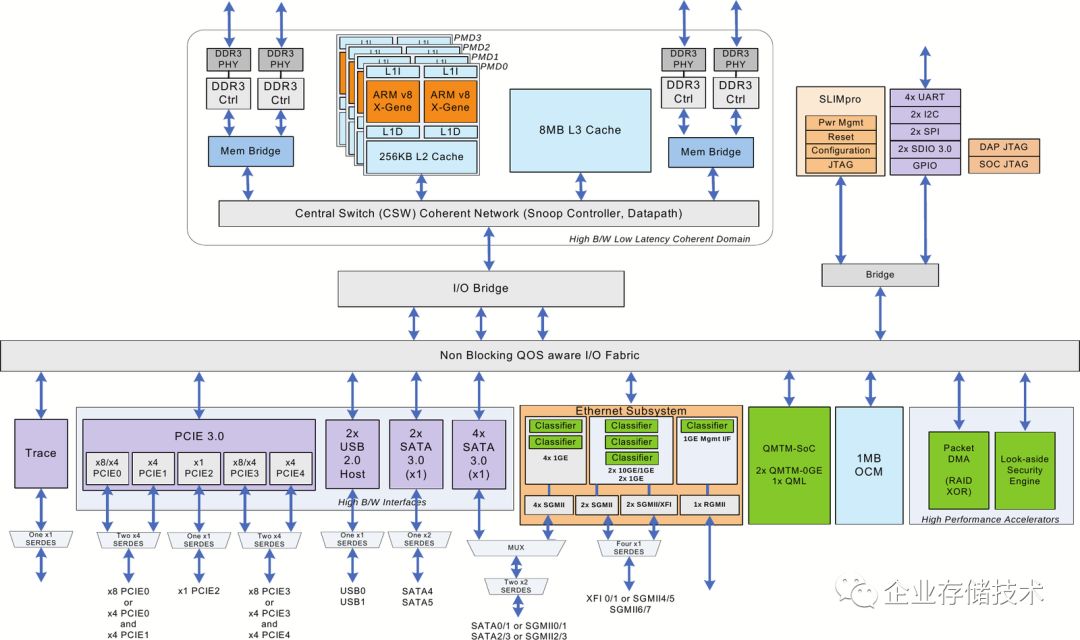
Figure 3.2 X-Gene’s framework diagram
I am most impressed by the MSLIM part of X-Gene, which consists of 4 A5 cores forming a small processor cluster that provides acceleration functionality. I am not sure if any customers used this processor group, nor do I know the design concept from back then.
From design to production, how many designs are overlooked by customers, and how many designs exceed expectations once in the hands of customers? I believe architects also feel confused; there are many uncertainties in the engineering world.
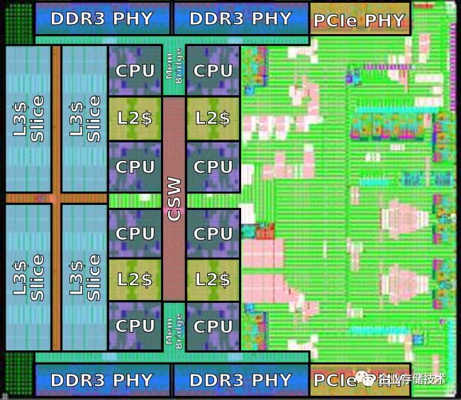
Figure 3.3 X-Gene die
Figure 3.4 X-Gene CPU module
There is no information on the entire die, but there is information on the processor module. Each processor module has 2 cores sharing L2, under 40nm process, 14.8 mm², 84M transistors. Based on this size, I estimate the entire die is about 300 mm2
Anandtech once had a detailed and quite negative review report. The central idea is that it is not yet mature, and the advantages in performance and efficiency are not obvious. It tested HPE’s moonshot system, while HPE’s official documentation actually rated X-gene quite highly, as it was the first mass-produced Arm 64bit server chip, and the initial software partners were all using its systems.
I knew about Applied Micro-APM when it was still called AMCC. The AMCC team is one of the few old teams in Silicon Valley that still makes CPUs, but they were making PowerPC. They faced difficulties in multi-core, so they switched to Arm to start over. Because they are an old CPU design team, they chose the most challenging route of architecture licensing and self-researched cores. I once argued with a colleague over this, saying, “I stand up as a man, and if I fall, I am still a man.” My male colleague laughed in anger and said, “Alright, you are a man.”
X-gene2 is essentially a 28nm tick implementation of X-gene1, nothing more.
3.1.1 eMAG-X-Gene3 2018
I hesitated for a long time, unsure whether to categorize this Ampere redesigned eMAG as the tail end of the second wave or the beginning of the third wave. Based on the core’s original design being derived from X-Gene 3, it is still considered the tail end of the second wave.
Figure 3.5 Ampere eMAG
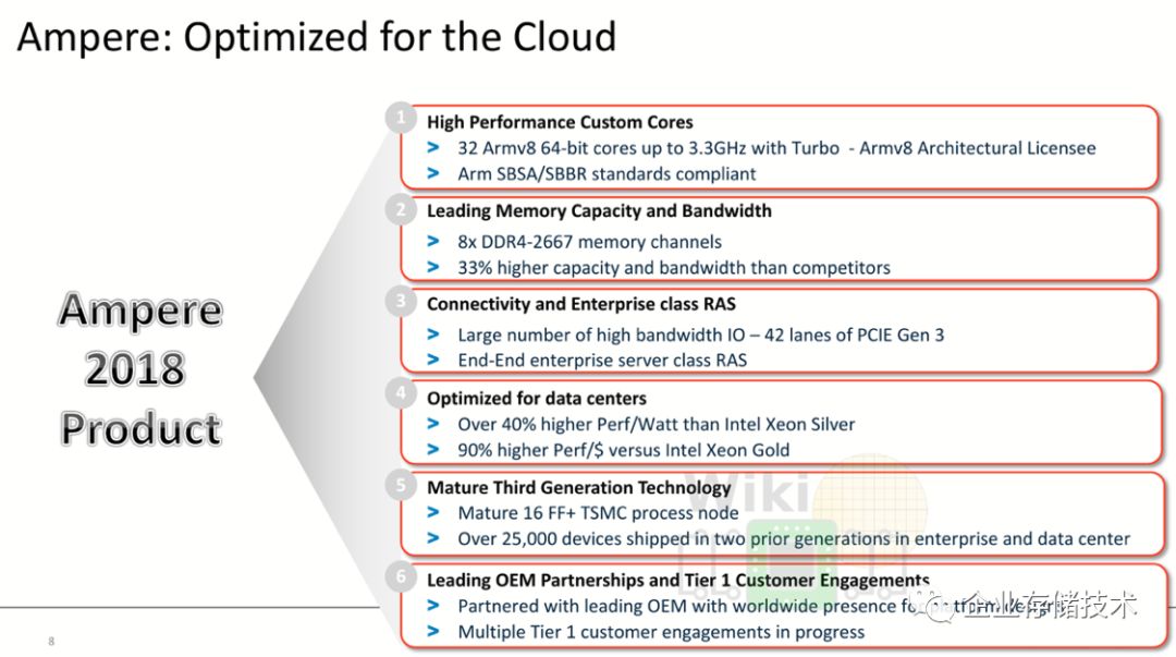
Figure 3.6 Ampere Product Advantages
32 cores list price is $850, a relatively competitive price. The framework diagram looks familiar; I won’t analyze it.
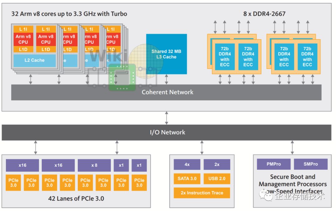
Figure 3.6 Ampere eMag Framework Diagram
3.2 AMD’s A1100 (2012)
One year after the launch of the Armv8 architecture, Arm released the A57 and A53 two cortex-A5x series products. According to international conventions, a heavyweight partner appeared at the launch event with Arm, which was AMD.
Internally codenamed Seattle, this chip belongs to the Opteron series, and the official product name later became A1100, a product no longer found in AMD’s main product history.
At that time, AMD spent a considerable amount of time explaining why to develop Arm servers and how to position the internal x86 and Arm product lines. To stabilize external doubts, they even launched the news-only K12 (2015).
If we look back at 2012, there is a term that cannot be ignored, “microserver”, and at that time, AMD had just acquired SeaMicro, a company focused on building high-density, low-power systems around the Freedom Fabric. This Fabric is very high density(very-high-density), low power; does it sound familiar? It’s Calexeda’s approach. The following image shows the 10U size, with 768 CPUs, including four GE switches and a load balancer.
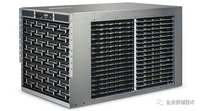
Figure 3.7 Calexeda 10U System
In such a system design, equipping a super low-power Arm processor makes much more sense. Therefore, it chose Arm’s standard core Cortex-A57, shortening development time and saving development costs, which is also a logical decision.
Documentation on Cortex-A57 is abundant worldwide, so I won’t list it here. As mentioned in the previous chapter, AMD chose a 2 core 4 cluster configuration, rather than the 4 core 2 cluster common in mobile AP. The benefits? You can experience it yourself.
The list price of this chip is $150, which is also quite competitive.
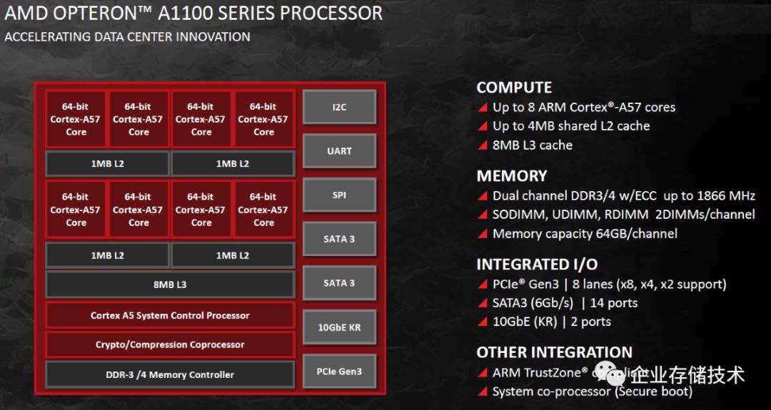
Figure 3.8 AMD Opteron A1100 Framework Diagram
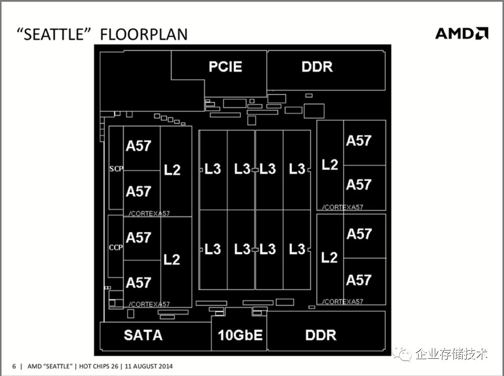
Figure 3.9 AMD Opteron A1100 Floorplan
In a sense, AMD’s Seattle is included in the second wave. Its design theory is entirely from the first wave, while K12 is the second wave.
However, looking at K12’s design goals, under AMD’s framework, the question of why to do Arm naturally leads to x86. Jim Keller was originally associated with K12, but… … this man is a free-spirited character.
Intel’s response to this wave was the 14nm “Xeon-D”.
3.3 Cavium ThunderX 2014
To some extent, Cavium’s 48 cores ThunderX is the product that truly opened the second wave of Arm server trends. It brought together all the characteristics that a mainstream server chip should have, such as dual-socket and performance.
Cavium, as a company only 1/10 the size of AMD, had the design capability for ultra-multi-core processors early on, but previously focused on MIPS network applications.
Although it has only 2 issue self-researched cores, its single-core performance is relatively weak. However, the overall SoC design, especially the multi-socket design, is excellent. Moreover, due to its accumulation in network processors, this chip has a rich array of acceleration engines and I/O interfaces.
Additionally, to reduce power consumption, it can selectively turn off acceleration engines, resulting in four different configurations: cloud computing version, storage version, operator version, and security version.
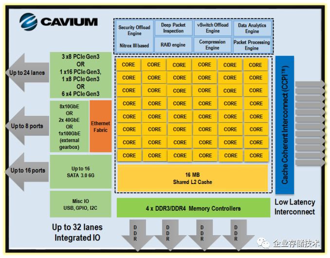
Figure 3.10 Cavium ThunderX Framework Diagram
Anandtech has a very good performance test, which helps to understand Cavium ThunderX.
3.4 Broadcom Vulcan ThunderX2
This is a complicated section. If we talk about Broadcom Vulcan, that was around 2016. If we talk about Cavium’s Thunder X2, that’s a product from 2018. Then it quickly became Marvell’s ThunderX2. Originally, these were products planned at the same time, but various twists turned them into one. Sometimes, I can hardly believe that our industry has so many dramatic stories.
Speaking of which, the CPU design team from RMI of Broadcom and Cavium’s CPU design team have many similarities; both are from the MIPS system and have a background in networking. However, unlike Cavium, which always made 2 issue small cores, the Broadcom team was adept at multi-threading from the start. Therefore, when planning, Vulcan was designed to be a 4-thread processor. At this time, there were no multi-threaded processors in the ARM camp.
Broadcom’s original design goal was 16nm, with a die size of 600 mm2, 32 cores, and each core supporting 4 threads, and dual P systems. After being acquired by Cavium, the die size was not disclosed.
The highest configuration, CN9980, has 32 cores, 2.5Ghz, and TDP of 200W. The 2.2Ghz, 180W CN9980 is priced at $1795, while the 16 core CN9960 runs at 1.6 Ghz and has a TDP of 75W priced at $800.
Its target market, or rather visible design win is concentrated in the HPC market.
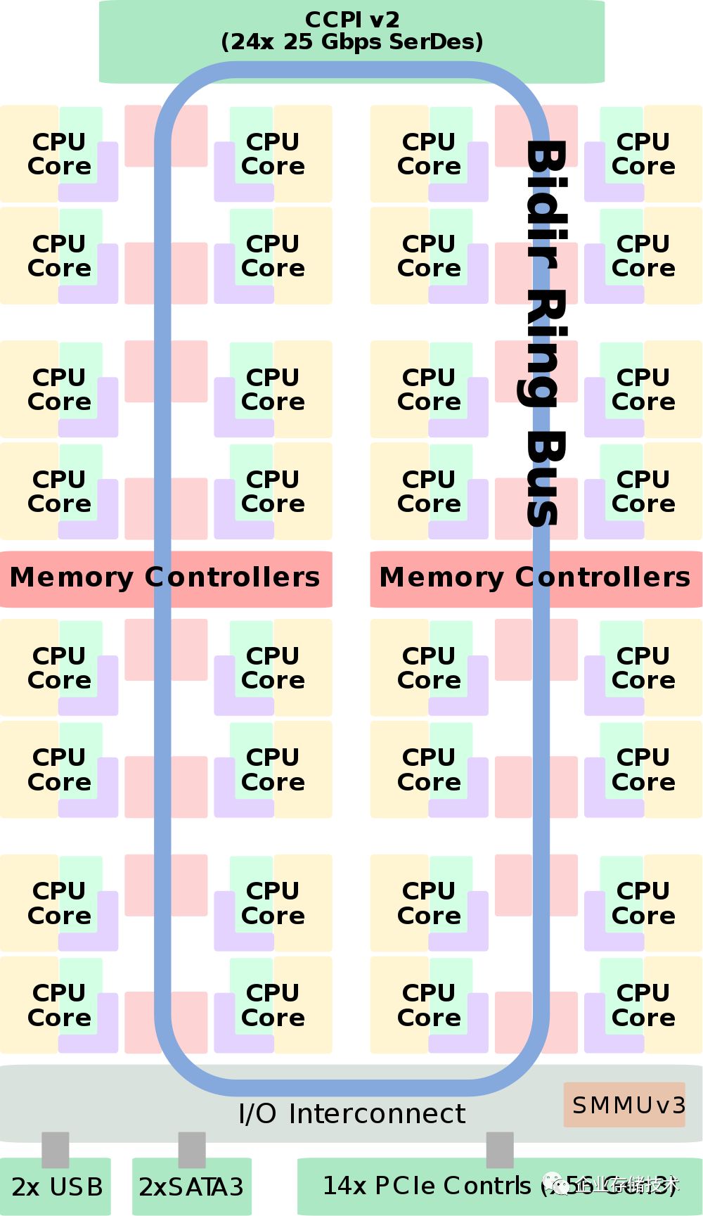
Figure 3.11 ThunderX2 Framework Diagram
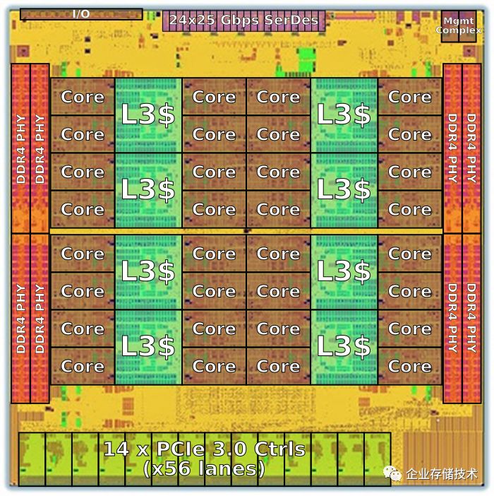
Figure 3.12 ThunderX 2 Layout
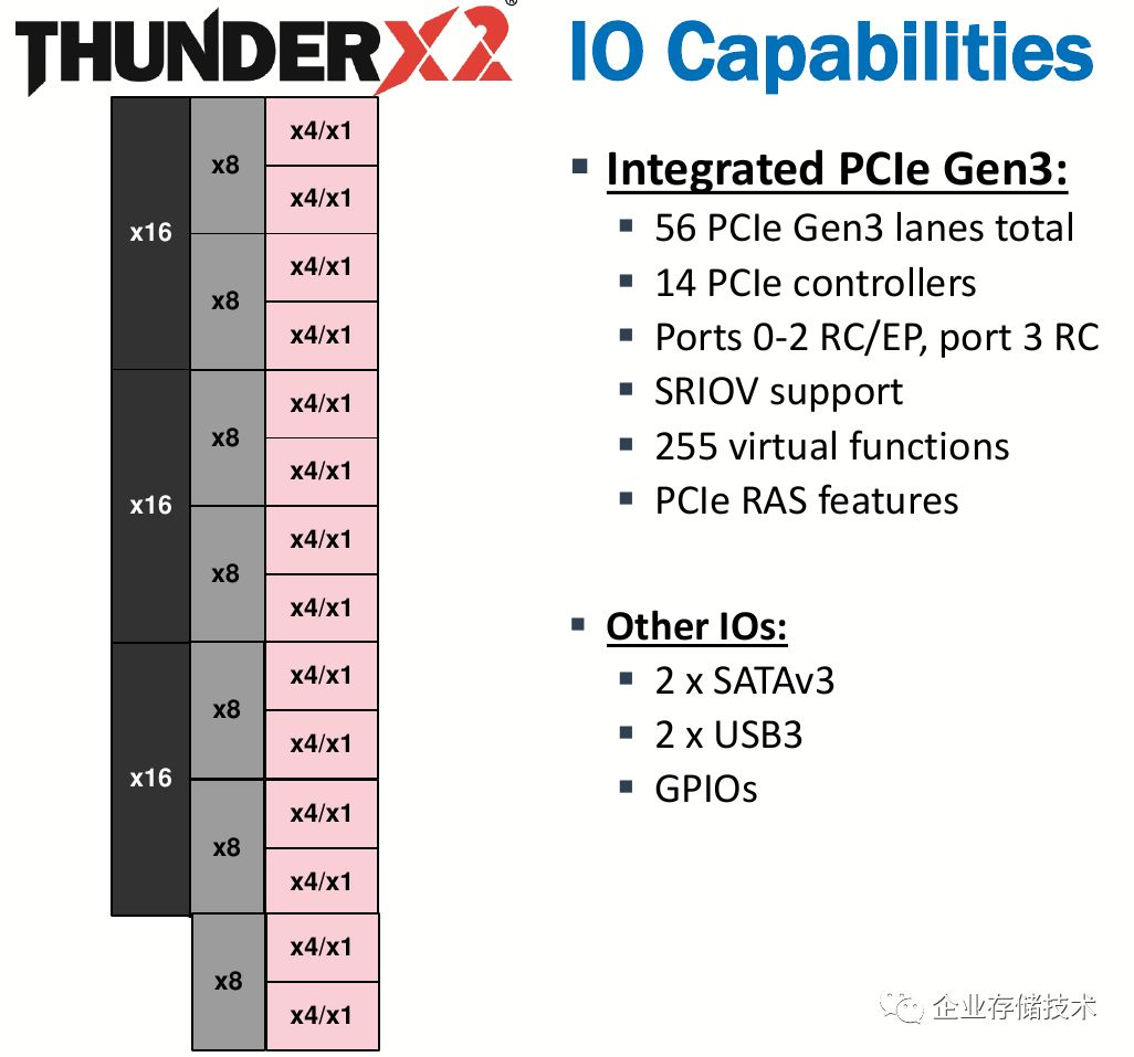
Figure 3.13 ThunderX2 IO Interfaces
3.5 Qualcomm 2017
In 2017, Qualcomm launched the original codename “ Amberwing” 48 core 10nm Centriq 2400 in the same week it received a $130 acquisition offer from Broadcom.
It is estimated that this Centriq 2400 took 4 years and cost between $100M and $125M, involving hundreds of engineers. During this period, Qualcomm also developed a 24 core Centric 1200 as a test prototype.
Centriq 2400 has 18B transistors, 398mm2, using Samsung’s 10nm process, making it much more compact than ThunderX2. Although it is a single P processor, this should not pose a problem given the development patterns of many generations of servers.
Figure 3.14 Centriq 2400
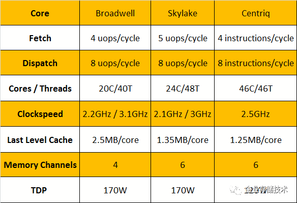
Figure 3.15 Centriq2400 Microarchitecture Comparison
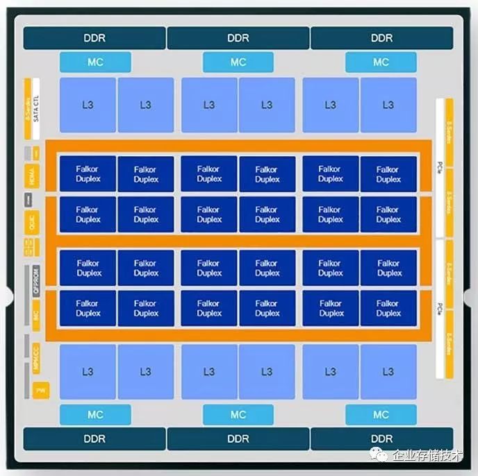
Figure 3.16 Centriq2400 Framework Diagram
This chip, born with a golden key, sailed smoothly to tape out, until the appearance of a black swan named Hock Tang.
From the price and power consumption table, Centriq2400’s pricing is basically consistent with ThunderX2.
The CPU core name of the Centriq 2400 is “Falkor,” which is Qualcomm’s fifth-generation self-researched core. If there were to be a next-generation core, it would be called “Saphira,” and the chip would be named “Firetail.” However, there was no next generation; Qualcomm canceled its server chip project, marking the end of the second wave of Arm server trends.
3.6 Samsung(2012-2014)
The main line is complete, but the side line must also be written.
Samsung’s Arm server story is little known in the country but has appeared in the Wall Street Journal. Samsung has never officially announced it; when the entire project started, everyone was guessing, and when it ended, everyone was still speculating.
In 2007, Samsung invested $3.5b to build a factory in Austin, and in 2010 established Samsung Austin Research Center and began hiring chip design engineers, later recruiting a VP from AMD to be the VP of Austin. The speculation was that server chips were also part of the plans at this Austin research center.
In fact, Samsung’s entry into server SoC design logic can be closely related to Qualcomm, but at that time Qualcomm had the support of the CEO and a dramatic ending, whereas a Korean company’s US branch trying to sustain a large server chip design is quite a challenge.
3.7 Nvidia Project Denver 2011-2014
Nvidia is a company I greatly respect, and it is one of the few companies in Silicon Valley still led by its founders as CEO. However, I have written this chapter several times without being able to finish it. This is likely because Nvidia remains a company primarily focused on GPUs, while its CPU development logic is more application-oriented and free-spirited.
This is a path from Tegra to Carmel, integrating Arm CPUs into complex function chips. In fact, it looks more like a system company’s chip planning path. Since this article focuses on the analysis of general server chips, otherwise Nvidia’s product line absolutely deserves a complete chapter analysis.
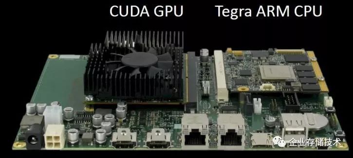
Figure 3.17 Tegra Arm CPU
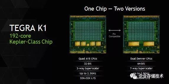
Figure 3.18 Eegra K1
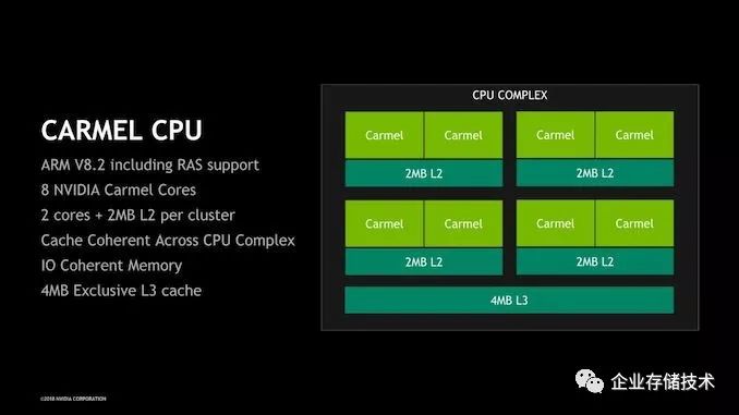
Figure 3.19 Carmel CPU
3.8 Balkal
The first 28nm chip in Russia, BE-M1000, should not be classified as a server chip, but it covers workstations. This chip company, like Japan’s Fujitsu and China’s Feiteng, also emerged from supercomputing projects and operates independently, focusing more on commercial success.
I once saw their ambitious roadmap. However, from roadmap to product landing, there are too many variables in the three to five years in between, leading to many dissipating aspirations.
Speaking of chip-making, this is a traditional strong point for supercomputing comrades. The previously mentioned server SoC also comes from the push of the supercomputing market. Later, I will mention that Europeans are also starting to strive to create their own chips.
Figure 3.20 Balkal BE-M1000
3.9 Phytium
Public information about Feiteng’s chips comes from hotchips 2015. The latest roadmap comes from Feiteng’s general manager Dou Qiang’s public sharing on December 19, 2019.
Details are not elaborated.
3.10 HiSilicon 1616
HiSilicon’s 1616 is the previous generation of Kunpeng 920, a relatively low-key generation. There is no introduction on Huawei’s official website. I won’t provide any external information.
Regarding HiSilicon, I feel that a historical epic could be written in the style of “Those Things About the Ming Dynasty,” followed by a biographical work titled “The Heroes of HiSilicon.” Writing about a company like HiSilicon from a liberal arts perspective is challenging; it requires someone like me, a literary youth with a scientific background. Everything is ready, just missing two things: one is the manuscript fee paid in advance by HiSilicon’s publicity department, and of course, crowdfunding from netizens can also be considered, and two is that I need to wait until I retire.
3.11 Socionext
Socionext’s chip