Conference Invitation
Artificial Intelligence (AI) Chip Design Seminar (July 25, Beijing National Convention Center)
A domestic startup specializing in AI FPGA acceleration algorithms, Deep Insight Technology, was acquired by the international giant Xilinx just two days ago, causing quite a stir in the industry. Currently, there are quite a number of companies in China working on AI chips, and AI chips have indeed become the hottest field in the chip industry today. However, most people may not be too familiar with the architecture of AI chips. So, what are the differences between AI chips and traditional chips? What is the architecture of AI chips like? To address this question, I have gathered some insights from industry experts on Zhihu and am now sharing them with you. Of course, to better understand the architecture of AI chips, it is best to attend the AI chip design seminar hosted by EETOP on July 25 at the National Convention Center. We are fortunate to have invited Professor Li Hongge, director of the Integrated Circuit Center at Beihang University, to give a keynote lecture on “Integrated Circuits and Brain-like Chip Architecture”. I believe everyone will gain a deeper understanding after the lecture.
Artificial Intelligence (AI) Chip Design Seminar (July 25, Beijing National Convention Center)

The following content is compiled from Zhihu:
Author: Wang Peng Link: https://www.zhihu.com/question/285202403/answer/444253962First, let me answer the question,
(1) There is a significant difference in performance compared to traditional chips, such as CPUs and GPUs. AI chips are faster and more energy-efficient when executing AI algorithms.
(2) The manufacturing process is the same; at least for now, everyone is the same.
The so-called AI chip generally refers to ASICs (Application-Specific Integrated Circuits) designed for AI algorithms.
Traditional CPUs and GPUs can also execute AI algorithms, but they are slow, have low performance, and cannot be practically commercialized.
For example, autonomous driving requires recognizing road pedestrians, traffic lights, and other situations. However, if a current CPU is used for calculations, it might not detect that there is a river ahead until the car has flipped into it, which is slow—time is life. If a GPU is used, it is indeed much faster, but it consumes a lot of power, and the car’s battery might not support normal use for long. Moreover, GPUs are very expensive, often costing over ten thousand yuan for a single unit, which ordinary consumers cannot afford, and they are often out of stock. Additionally, since GPUs are not specifically developed as ASICs for AI algorithms, their speed has not reached its limit, and there is still room for improvement. In fields like intelligent driving, speed is essential! In mobile terminals, AI applications like face recognition and voice recognition must have low power consumption, so GPUs are out!
Therefore, the development of ASICs has become inevitable.
Now, let’s discuss why AI chips are needed.
AI algorithms, especially in fields like image recognition, often use CNN (Convolutional Neural Networks), while in speech recognition and natural language processing, RNN (Recurrent Neural Networks) is mainly used. These are two distinct types of algorithms. However, they are essentially matrix or vector multiplications and additions, combined with some divisions, exponentials, and other algorithms.
A mature AI algorithm, such as YOLO-V3, involves a large number of convolutions, residual networks, and fully connected layers, fundamentally consisting of multiplications and additions. For YOLO-V3, if the specific input image size is determined, the total number of multiplication and addition calculations is fixed. For example, it could be a trillion times (the real situation is much larger).
To quickly execute YOLO-V3, it must complete a trillion addition and multiplication operations.
At this point, let’s look at IBM’s POWER8, one of the most advanced superscalar CPUs, running at 4GHz, SIMD, 128bit. Assuming it processes 16bit data, that means 8 numbers, so in one cycle, it can perform at most 8 multiply-add calculations. In total, it can perform a maximum of 16 operations at once. This is still theoretical, and practically, it is unlikely to achieve.
So, the peak calculation times of a CPU in one second = 16X4Gops = 64Gops.
Now, let’s calculate the time it takes for a CPU to perform one calculation.
Similarly, if we switch to a GPU, we can determine the execution time as well. Due to unfamiliarity with the internal structure of GPUs, I won’t go into specific analysis.
Next, let’s talk about AI chips. For example, the famous Google TPU1.
TPU1 runs at about 700MHz and has a 256X256 size pulse array, as shown in the figure below. In total, there are 256X256=64K multiply-add units, each capable of executing one multiplication and one addition at a time, resulting in 128K operations (counting multiplication as one and addition as another).
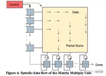
Additionally, besides the pulse array, there are other modules, such as activation functions, which also include multiplications and additions.
Therefore, the peak calculation times of TPU1 in one second is at least = 128K X 700MHz = 89600Gops = approximately 90Tops.
Comparing the CPU and TPU1, we find a difference of several orders of magnitude in computing power, which is why CPUs are considered slow.
Of course, the above data are entirely ideal theoretical values; in practice, it might reach only about 5%. This is because the storage on the chip is not large enough, so data is often stored in DRAM, which is slow to access, causing the multiplication logic to often be idle. Additionally, AI algorithms consist of many layers of networks that must be calculated layer by layer, so when switching layers, the multiplication logic is also idle. These various factors lead to the actual chip not reaching its theoretical peak performance, and the gap is significant.
Some may argue that research can tolerate slower processing.
Currently, the size of neural networks is increasing, and the number of parameters is growing. When dealing with large NN models, training can take weeks or even months. Will you be patient enough to wait? What if there is a sudden power outage, and everything has to start over? (I once trained an AI to write novels, and one training session (50 epochs) took about a day and a night. I remember starting the training in the morning and finishing the next afternoon, and that was for a relatively simple model with only tens of thousands of data points.)
After modifying the model, it takes several weeks to know the results. Can you afford to wait?
With the sudden availability of TPU, you might find that you can optimize parameters and continue running just after returning from lunch—how enjoyable that is!
Fast computation speeds enable rapid iterations, leading to the development of stronger AI models. Speed is money.
Since I am unfamiliar with the internal structure of GPUs, I won’t compare them. What is certain is that GPUs are still relatively fast, at least much faster than CPUs. Therefore, most people currently use GPUs, which often cost over ten thousand yuan, are very expensive, and have high power consumption, making them unsuitable for large-scale use in data centers.
In summary, CPUs and GPUs are not AI-specific chips; to implement other functions, they contain a lot of additional logic that is completely unnecessary for current AI algorithms, leading to suboptimal performance and cost-effectiveness.
Google has invested in developing TPU and has now released TPU3, which is being used quite well and supports Google Cloud computing services, reportedly at around $6 per hour, though I don’t remember the exact unit, and I’m too lazy to check.
This shows that Google believes it is necessary to develop TPU independently.
Currently, the most accurate algorithms in fields like image recognition, speech recognition, and natural language processing are based on deep learning. The computational accuracy of traditional machine learning has already been surpassed, and the most widely used algorithms today are undoubtedly deep learning. Additionally, the computational load of traditional machine learning is much lower compared to deep learning. Therefore, when discussing AI chips, I focus on deep learning algorithms that require substantial computation. After all, for algorithms with smaller computational loads, CPUs are already quite fast. Moreover, CPUs are suitable for executing complex scheduling algorithms, which GPUs and AI chips cannot achieve. Thus, the three types of chips are only targeting different application scenarios, each with its own strengths.
As for why I compared CPUs instead of specifically mentioning GPUs,
it is because, as I mentioned, I currently have not systematically reviewed GPU-related papers and am not familiar with the situation regarding GPUs, so I won’t analyze them. Due to familiarity, I chose to compare with superscalar CPUs. Moreover, small networks can be trained entirely using CPUs without any significant issues, just a bit slower, as long as the network model is not too large.
For AI algorithm companies like SenseTime and Megvii, their models are large, and naturally, they cannot be handled by a single GPU. The computing power of GPUs is also quite limited.
Regarding the statement that CPUs are serial and GPUs are parallel,
that is correct, but it is not comprehensive. I will just mention that the CPU I referred to is IBM’s POWER8, which is a top-tier server CPU with a frequency of 4GHz. I wonder if you noticed that I mentioned it is SIMD? This SIMD means it can execute multiple identical instructions simultaneously, which is parallel processing, not serial. A single data point is 128bits, and if the precision is 16bits, then theoretically, in one cycle, it can calculate up to eight groups of multiplication or addition or multiplication-addition. Isn’t that parallel? It is just that the degree of parallelism is not as powerful as that of GPUs, but it is still parallel.
I’m not sure why CPUs cannot be used for comparison of computing power.
Some comments highly praise GPUs, claiming that comparing with CPUs is inappropriate.
Come on, GPUs were originally separated from CPUs specifically to handle image calculations, which means GPUs are designed to handle image computing, including various display effects. This is also a natural flaw of GPUs; they are more targeted at rendering and other computational algorithms. However, these algorithms differ significantly from deep learning algorithms, and the AI chips I mentioned, such as TPUs, are specifically developed for typical deep learning algorithms like CNNs. Additionally, Cambricon’s NPUs are also specifically designed for neural networks, similar to TPUs.
When Google’s TPU was first introduced, comparisons were made with CPUs and GPUs.
For instance, the abstract of Google TPU’s paper directly compared the performance of TPU1 with CPUs and GPUs, as shown in the red box:
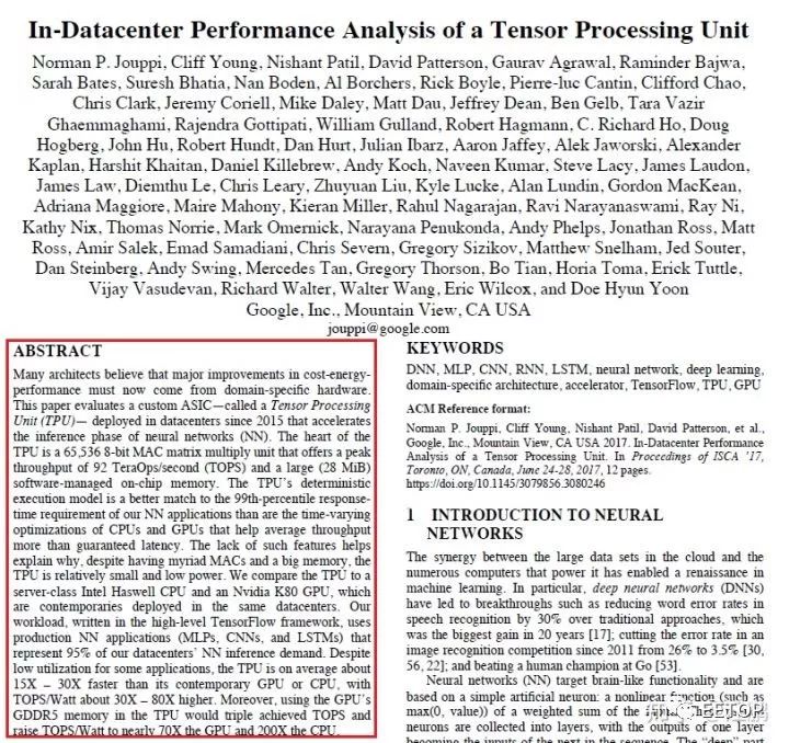
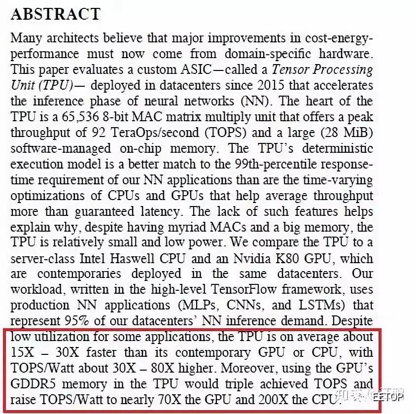
This is the performance comparison of TPU1 with CPUs and GPUs presented in the abstract.
Now let’s take a look at Cambricon’s DianNao paper, where the abstract directly compares the performance of DianNao with CPUs, as shown in the red box:
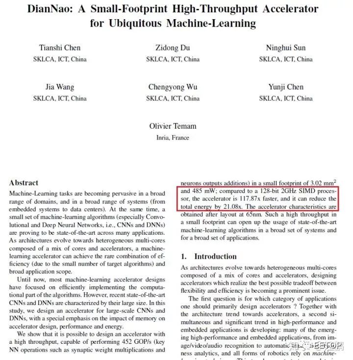
Looking Back at History
When neural networks first appeared in the last century, they were computed using CPUs.
When Bitcoin first emerged, it was also mined using CPUs. It has now evolved into ASIC mining machines, which you can learn about from Bitmain.
Since the deep learning boom began in 2006, both CPUs and GPUs could compute, and it was found that GPUs were faster, but they were expensive; thus, more CPUs were used. At that time, GPU’s CUDA was not very mature. Later, as NN models grew larger, the advantages of GPUs became more apparent, and CUDA became increasingly powerful, leading to the current GPU dominance.
Cambricon’s DianNao (NPU) released in 2014 is faster than CPUs and more energy-efficient. The advantages of ASICs are evident, which is why they are being developed.
As for many companies’ solutions being programmable, most are based on FPGAs. Are you referring to SenseTime and Deep Insight? Indeed, the papers they published are based on FPGA.
These startups primarily focus on research algorithms; the chips are not their main focus, and they currently do not have the energy or capability for that. FPGAs are very flexible, low-cost, and can quickly implement architectural design prototypes, so they naturally choose FPGA-based solutions. However, recently, they have been heavily financing, and their websites are also recruiting for chip design positions, so they are likely venturing into ASIC development.
If FPGA-based programmable solutions truly have immense commercial value, why would they spend money developing ASICs?
Having said all this, I am also a newcomer to this field, learning out of necessity for work. Based on my current understanding, by examining TPU1’s patents and papers, I can derive its internal design methods step by step. Understanding TPU1 gives insight into most of what is considered an AI processor. Then, studying Cambricon’s series of papers reveals several different architectures for different situations, which may be worth researching. There are also other unicorns like SenseTime and Deep Insight Technology, which publish papers annually, and it would be beneficial to keep an eye on those. These papers likely represent the most advanced AI chip architecture designs currently available. Of course, the most advanced designs are not publicly disclosed; for instance, Google has not released patents related to TPU2 and TPU3, at least I haven’t found them. However, the current literature already represents the most advanced progress in recent years.
Author: Bluebear
Link: https://www.zhihu.com/question/285202403/answer/444457305
The AI chips currently being discussed can be divided into two categories: one category is for both training and inference, which can be handled by GPGPU, CPU, and FPGA (like Altera’s Stratix series). However, Google’s TPU2 and Bitmain’s Sophon, designed specifically for these tasks, may have advantages in energy efficiency. This category has fewer players but is more interesting. Of course, ICLR also has work exploring training with fixed-point devices, and Xilinx hopes that XNOR-net will allow fixed-point devices to participate in training.
The other category is Inference Accelerator chips, which simply run pre-trained models on chips. This area is truly flourishing, with products like Cambricon’s NPU, Intel’s Movidius (which also has a Nervana-like XeonPhi for training), Deep Insight’s DPU, Horizon’s BPU, Imagination’s PowerVR 2NX, ARM’s Project Trillium, and many others. These products include both standalone products and IP offerings for other developers to integrate deep learning accelerators into SoCs. Additionally, I should mention the Tegra X2, which is akin to a small desktop platform, combining ARM processors with Nvidia GPUs to provide complete training and inference capabilities, although it also has high power consumption. I believe other accelerator chips can be further divided into two categories: floating-point and fixed-point. The floating-point category includes only FP16 half-precision, but supports both FP16 and INT8, like Cambricon’s NPU and Intel’s Movidius. The fixed-point category includes purely fixed-point devices, such as Horizon’s BPU and Imagination’s PowerVR 2NX. There are also mixed options, which I will elaborate on later.
First, regarding non-ASICs, some Deephi products use ZYNQ, which saves on tape-out costs, using DSP48 and resources to implement multipliers for fixed-point operations, while floating-point operations are handled by the Cortex A9 hard core. Deephi mainly works on model pruning and quantization. I previously discussed with Professor Wang Yu that during network quantization, some layers experience significant quantization loss, hence retaining some layers (mainly the last one) in floating-point format. Conversations with those working on acceleration at Bitmain have confirmed this; using SOPC is relatively straightforward. Additionally, hybrid solutions, such as Qualcomm’s AI platform, utilize Adreno GPUs and Hexagon DSPs (mainly DSPs, which seem to have better energy efficiency than the 970), with SNPE primarily using OpenCL to leverage GPU and DSP resources for inference. MTK and AAPL have similar approaches. Other differences can be substantial; Intel’s Movidius was released earlier, supporting floating-point inference, and it actually contains VLIW SIMD units, which are similar to previous ATi graphics cards or DSP designs. I don’t have much public information regarding others, so I’ll just make some general observations. Generally, AI accelerators are optimized for existing networks, focusing on fixed-point or floating-point computations, primarily by stacking computing units (matrix compute units, multipliers) and reducing memory data transfer. The 970 may be connected to CCI and relies on significant caching, while PowerVR 2NX seems to be optimized for a 4-bit memory controller. By optimizing memory data pathways, they reduce some memory bandwidth requirements. Overall, these products are somewhat akin to ultra-multicore DSPs, albeit simplified, as DSPs can still handle some control tasks, which is not the case for GPUs and AI chips.
In another sense, they are poorly optimized for new networks; typically, industry lags behind academia by over a year. For example, DenseNet has emerged, but chips only support up to ResNet.
Regarding the following two questions:
If GPGPU or CPU performs inference, the energy efficiency won’t look good. However, floating-point inference is generally more accurate than fixed-point or reduced precision situations (though there are cases where fixed-point quantization generalizes well). However, if an NPU can only perform specific tasks under CPU control, it is quite embarrassing; without many applications supporting it, NPUs become quite useless. In mobile devices, many times you simply do not need an NPU, so I think using Mali or similar would suffice…
There is no difference; they use the same manufacturing processes as other chips like mobile SoCs and GPUs. If you have the budget, you can use new processes and technologies.
Author: DeepTech
Link: https://www.zhihu.com/question/285202403/answer/446703288
What can artificial intelligence bring to our lives? Taking our most familiar mobile phones as an example, daily photo beautification has become commonplace. However, current selfie software requires uploading to the cloud after shooting to complete “one-click beautification” through a general model. In contrast, mobile AI chips can synchronize photo beautification right after (or even during) the shooting process based on user preferences, which is challenging for existing CPUs.
So, what are the differences? First, traditional chips only need to call the corresponding system to work based on instructions during computation, while AI instructions contain a considerable amount of parallel computation and modeling. This undoubtedly places high demands on the processor’s computational capability.
Secondly, there is the data collection capability of mobile devices, especially smartphones. Excellent AI applications require collecting vast amounts of data to train models, and smartphones are undoubtedly the best data collection tools. With an increasing number of sensors, such as microphones, cameras, gravity sensors, and location devices, an AI chip capable of real-time collection, synchronous processing, and connecting different sensors becomes particularly important.
Of course, an AI chip integrating over 5.5 billion transistors in an area the size of a fingernail cannot be limited to simple photography. Currently, smartphones already have intelligent applications for voice services, machine vision recognition, image processing, and will likely expand to include more diverse applications, including medical, AR, and gaming AI.
In addition to satisfying applications on mobile devices, future AI chips will also have opportunities to expand into other more promising markets. A typical example is autonomous driving; Tesla poached AMD’s legendary architect Jim Keller last year to develop its own AI chip. In the future, whether for rockets or deep-sea explorers, the control systems they rely on will increasingly become AI-driven.
Conference Invitation
Artificial Intelligence (AI) Chip Design Seminar (July 25, Beijing National Convention Center)


Click to read and register for the AI chip seminar