Please click to view the complete disassembly process.
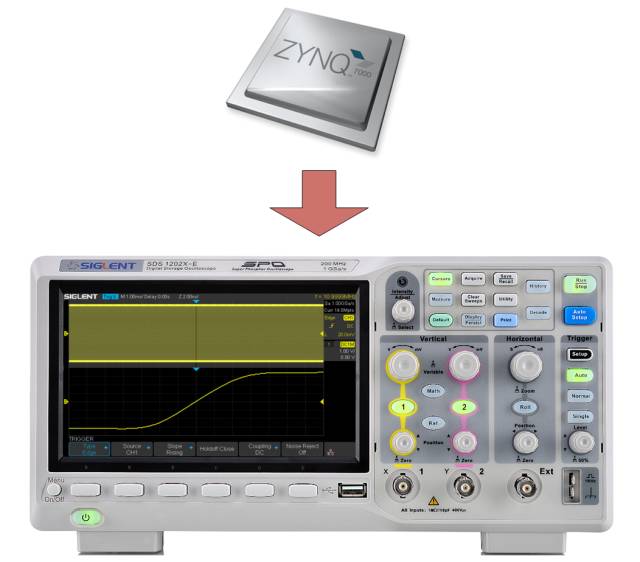
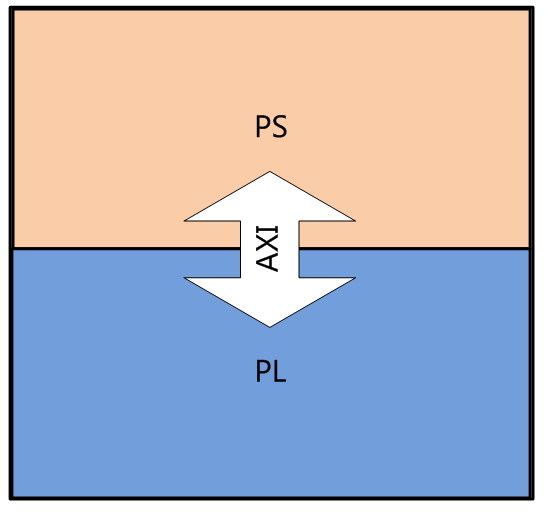
△Figure 1 The SDS1000X-E integrates the Zynq-7000
The SDS1000X-E uses the XC7Z020 SoC chip, which features a dual-core ARM Cortex-A9 processor (PS) + FPGA based on the Artix-7 architecture (PL). The processor part supports a maximum clock frequency of 866 MHz, while the FPGA part includes 85k logic cells, 4.9 Mb Block RAM, and 220 DSP Slices, providing support for commonly used external memory such as DDR2/DDR3, which is very suitable for the needs of data acquisition, storage, and digital signal processing in digital oscilloscopes. At the same time, the PS (processor system) and PL (programmable logic) parts of the Zynq-7000 are interconnected via a high-speed AXI bus, effectively solving the bandwidth bottleneck problem of data transmission between the CPU and FPGA in traditional digital storage oscilloscopes, which is beneficial for reducing the dead time of digital oscilloscopes and improving waveform capture rates. Replacing traditional CPU + FPGA discrete solutions with a single SoC chip can also reduce hardware board area, facilitating the integration of high-performance processing systems into compact entry-level oscilloscopes.
Data Acquisition and Storage
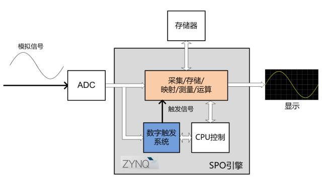
△Figure 2 The SPO engine built on the Zynq-7000 architecture
The high-speed ADC chip used in the SDS1000X-E has a data interface in the form of LVDS differential pairs, with a rate of 1 Gbps for each pair of LVDS. The Zynq-7000 chip supports a maximum LVDS rate of 1.25 Gbps for programmable IO, ensuring stable and reliable reception of data sampled by the ADC.
At the same time, the high-speed ADC data received by the FPGA needs to be written to memory in real-time. For an 8-bit, 1 GSa/s ADC, the output data throughput rate is 1 GByte/s. Zynq-7000 supports commonly used low-cost memory such as DDR2 and DDR3, with a maximum DDR3 interface rate of 1066 MT/s, so using a single DDR3 can meet the real-time storage requirements of the aforementioned ADC output data. Moreover, the Zynq-7000 supports PL sharing the memory of PS, as long as enough memory bandwidth is reserved for the PS part, the remaining bandwidth can be used to store ADC data without the need to add external memory in the PL part, reducing costs.
More importantly, based on the rich programmable logic resources in the Zynq-7000 (85k equivalent logic cells in XC7Z020), the SDS1000X-E integrates a highly sensitive, low jitter, zero temperature drift digital triggering system, making its triggering more accurate; various intelligent triggering functions such as slope, pulse width, video, timeout, underflow, code pattern, etc., can help users more precisely isolate the waveforms of interest; bus protocol triggering can even directly use qualified bus events (such as the start bit of the I2C bus, or specific data of UART) as trigger conditions, greatly facilitating debugging.
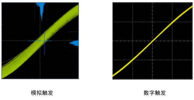
△Figure 3 Comparison of triggering jitter between analog triggering system and digital triggering system
Data Interaction
As the design complexity of digital oscilloscopes increases and the processing power of processors improves, the bus structure increasingly becomes a bottleneck in system performance. Traditional entry-level digital oscilloscopes use low-cost embedded processors as the control and processing core, employing low-cost FPGAs for data acquisition and storage, interconnected by a parallel local bus, with the processor as the master device and the FPGA as the slave device; other peripheral devices such as FLASH, USB controllers, etc., are also connected to the bus, as shown in Figure 4.
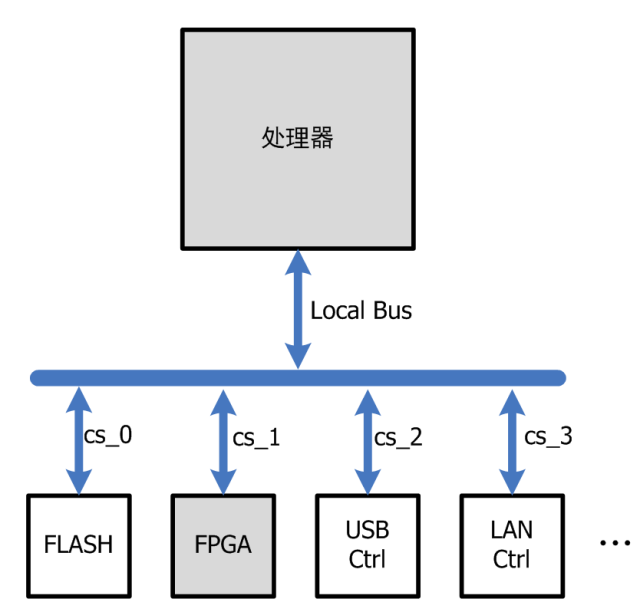
△Figure 4 Interconnection of traditional embedded processors and FPGAs
The biggest problem with this interconnection method is the low data throughput rate; first, because local buses are generally asynchronous, ideally, a read/write access requires at least 3 cycles (1 setup cycle, 1 access cycle, and 1 hold cycle). Taking a 16-bit wide local bus with an external bus frequency of 100 MHz as an example, its ideal maximum bus access throughput rate is 66 MB/s; second, because read and write operations share a set of address and data buses, it is a half-duplex operation; third, multiple slave devices compete for the bus, thus reducing the effective data throughput rate of each slave device. For a digital oscilloscope with a sampling rate of 1 GSa/s, the time to sample 10 M points is only 10 ms, but the time required to transmit 10 M points (taking the ideal 66 MB/s bus throughput rate as an example) is at least 150 ms, which is 15 times the data sampling time. In other words, even without considering data processing time, the dead time reaches 15/16 = 93.75%.
The SDS1000X-E adopts the Zynq SoC architecture, with a high-speed AXI bus interconnection between the processor (PS) and FPGA (PL), effectively solving the bandwidth bottleneck problem of data transmission between the two, greatly improving data throughput and reducing the dead time of the oscilloscope. The Zynq-7000 uses 4 AXI-HP ports, each of which supports a maximum 64-bit width and a clock frequency of up to 250 MHz; at the same time, the read and write channels are separated, allowing for full-duplex operation; the point-to-point transmission between PS and PL does not involve bus competition with other devices. Using a single HP port for data transmission, the throughput can easily reach a bidirectional speed of 1 GB/s, with a total read and write rate exceeding 8 GB/s across 4 ports, far exceeding the transmission rate of the local bus.
△Figure 5 Interconnection between processor and programmable logic in Zynq SoC
Digital Signal Processing
The SDS1000X-E is equipped with many practical and powerful digital signal processing functions, such as FFT supporting 1 M points of computation, enhanced resolution (Eres), serial protocol decoding with 14 M full sample points, various measurements, and mathematical operations, greatly enhancing the digital signal processing capabilities of entry-level digital oscilloscopes.
The rich hardware resources of the Zynq-7000 provide strong support for the digital signal processing functions of the SDS1000X-E. The XC7Z020 SoC chip used in the SDS1000X-E features a dual-core ARM Cortex-A9 processor with a maximum clock frequency of 866 MHz, and a parallel coprocessor NEON can perform digital signal processing at the software level; the PL part has 220 DSP Slices and 4.9 Mb Block RAM; combined with the high throughput of the data interface between PS and PL, we can flexibly allocate different hardware resources for various digital signal processing tasks.
Complex computation instructions suitable for software implementation can be executed on the PS side, such as measuring the rising edge of the signal; functions that require a large number of multiply-accumulate operations and rely heavily on hardware resources can be implemented on the PL side, such as interpolation filtering commonly used in oscilloscopes.
Some complex functions can leverage the high data bandwidth between PS and PL for collaborative processing, such as FFT computation, where the PL side utilizes abundant DSP Slices and Block RAM resources to construct a coprocessor for hardware acceleration of basic FFT operations, while the PS side performs complex window function calculations, plotting, UI operations, etc. Based on this collaborative processing architecture, the SDS1000X-E supports FFTs of up to 1M points, achieving extremely high spectral resolution while greatly accelerating the refresh speed of the spectrum. Figure 6 shows a comparison of spectral resolution for 16 k points and 1 M points FFT performed on the SDS1000X-E. In this example, we input a dual-tone signal with frequencies of 100 MHz and 100.05 MHz into the oscilloscope. The spectrum obtained from the 16 k points FFT does not allow us to distinguish these two closely spaced sine signals, which are displayed as a single frequency; however, the spectrum from the 1 M points FFT shows a significantly finer spectrum and signal processing gain, as seen from the graph expanded 100 times horizontally, where the two sine signals spaced 50 kHz apart can be well differentiated.
△Figure 6 1M points FFT achieves extremely high spectral resolution
Similarly, the SDS1000X-E has many high-performance digital signal processing functions achieved through collaborative processing between PS and PL. For example, the SDS1000X-E can perform various measurements and serial protocol decoding on 14 M full sample points, which is not achievable in many mid-range and high-end oscilloscopes. In Figure 7, the upper two images show the measurement results of a certain mainstream mid-range oscilloscope for a 10 ns rising edge, while the lower two images show the measurement results of the SDS1000X-E for the same signal. It can be seen that at small time bases, the measurement results of both are quite accurate and do not differ much from the actual rise time. However, at larger time bases, the upper right image shows that this oscilloscope can only display a measurement result of “< 48ns” at 100 us/div, while its original sampling rate still has 1 GSa/s. This indicates that its measurement target is not the original waveform data, but rather the data mapped to the screen after compression. The lower right image shows the measurement results of the SDS1000X-E at a time base of 1 ms/div, noting that the sampling rate is also 1 GSa/s, but the displayed measurement accuracy still reaches 1 ns, accurately reflecting the parameters of the signal.
The SDS1000X-E, based on full sample point digital signal processing and a storage depth of up to 14 M points, allows users to observe the overall signal at large time bases while still obtaining detailed processing results; at the same time, its processing method based on the Zynq architecture optimizes the performance and speed of signal processing, providing better real-time performance and flexibility.
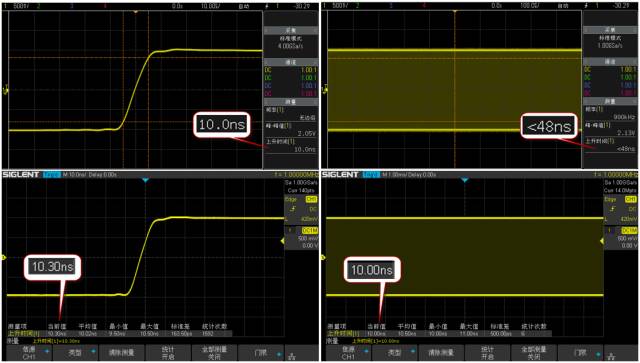
△Figure 7 Comparison of point measurement with compressed points and full sample points measurement accuracy
About SDS1000X-E
The SIGLENT SDS1000X-E series super phosphor oscilloscopes come in 70M, 100MHz, and 200MHz bandwidth models, with a sampling rate of 1 GSa/s and a standard storage depth of up to 14 Mpts. Most commonly used functions are designed with user-friendly one-button operation; employing SPO technology, it offers excellent signal fidelity: the bottom noise is lower than similar products in the industry, with a minimum range of only 500 μV /div; the innovative digital triggering system has high triggering sensitivity and low triggering jitter; waveform capture rates reach up to 400,000 frames per second (Sequence mode), with 256 levels of brightness and color temperature display; supports rich intelligent triggering, serial bus triggering, and decoding; supports history mode (History), sequence mode (Sequence), and enhanced resolution mode (Eres); equipped with rich measurement and mathematical operation functions; the 1M points FFT can achieve very detailed frequency resolution; the 14M full sample point measurement ensures that measurement accuracy and sampling accuracy are the same, with no distortion; it is a high-performance economical general-purpose oscilloscope.
About Zynq-7000
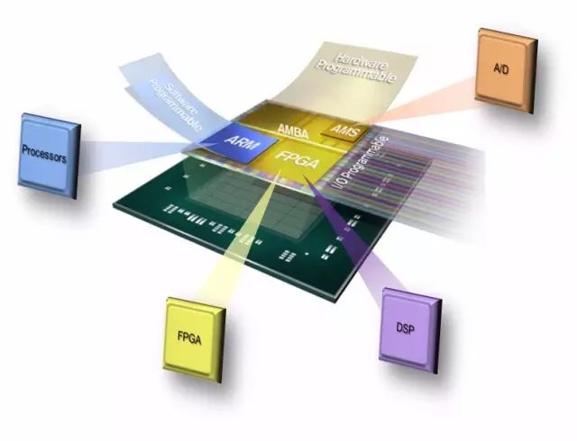
The Xilinx Zynq®-7000 All Programmable SoC (AP SoC) series integrates the software programmability of ARM® processors with the hardware programmability of FPGAs, enabling not only important analysis and hardware acceleration but also highly integrating CPU, DSP, ASSP, and mixed-signal functions on a single device. Zynq-7000 devices are equipped with dual-core ARM Cortex-A9 processors, which are integrated with programmable logic based on 28nm Artix-7 or Kintex®-7, achieving excellent performance-to-power ratios and maximum design flexibility.
About AXI Bus
AXI (Advanced eXtensible Interface) is a bus protocol proposed by ARM, which is the most important part of the AMBA (Advanced Microcontroller Bus Architecture) protocol. It is a high-performance, high-bandwidth, low-latency on-chip bus. Its address/control and data phases are separated, supporting unaligned data transfers. In burst transfers, only the starting address is needed, while the separated read and write data channels support Outstanding transfer access and out-of-order access, making timing convergence easier. AXI is a new high-performance protocol in AMBA. AXI technology enriches the existing AMBA standard content, meeting the needs of ultra-high performance and complex system-on-chip (SoC) designs.