“STM32F4xx timers are categorized into three types: advanced, general-purpose, and basic, featuring rich functionalities including timing, counting, and PWM. Advanced timers include motor control features, general-purpose timers support various capture and compare functions, while basic timers are used for simple timing. This article introduces their configuration and applications to help master development.”
01
—
Introduction to STM32 Timer
The timers in the STM32F4xx series microcontrollers are one of the core functional modules, providing flexible and diverse timing, counting, and PWM control capabilities. The STM32F4xx includes 14 timers divided into three main categories: advanced, general-purpose, and basic, with the main differences shown in the table below:
|
Feature |
Advanced Timer |
General Timer |
Basic Timer |
|
|
Timer Number |
TIM1, TIM8 |
TIM2~TIM5 |
TIM9~TIM14 |
TIM6, TIM7 |
|
Counter Bit Width |
16 bits |
16 bits (TIM3, TIM4) or 32 bits (TIM2, TIM5) |
16 bits |
16 bits |
|
Counting Direction |
Up / Down / Center Aligned |
Up / Down / Center Aligned |
Up |
Up |
|
Trigger Events |
Update, Trigger Event, Input Capture, Output Compare, Break Input |
Update, Trigger Event, Input Capture, Output Compare, Break Input |
Update, Trigger Event (only TIM9 and TIM12), Input Capture, Output Compare |
Counter Overflow |
|
DMA Output |
✅ |
✅ |
✅ (only TIM10, TIM11, TIM13, TIM14) |
✅ |
|
PWM Complementary Output |
✅ |
❌ |
❌ |
❌ |
|
Dead Time Control |
✅ |
❌ |
❌ |
❌ |
|
Brake Function |
✅ |
❌ |
❌ |
❌ |
|
Number of Channels |
4 Outputs + Complementary Outputs |
2~4 Outputs |
2 (TIM9 and TIM12) or 1 (TIM10, TIM11, TIM13, TIM14) |
None |
|
Channel Waveform |
Input Capture, Output Compare, PWM Generation, One Pulse Mode Output |
Input Capture, Output Compare, PWM Generation, One Pulse Mode Output |
Input Capture, Output Compare, PWM Generation, One Pulse Mode Output |
None |
|
Encoder Interface |
✅ |
Partially Supported (TIM2~5) |
❌ |
❌ |
|
External Clock Trigger Input |
✅ |
✅ |
❌ |
❌ |
|
Per Cycle Current Management |
✅ |
✅ |
❌ |
❌ |
|
Typical Applications |
Motor Control, Power Management |
PWM Generation, Event Counting |
PWM Generation, Event Counting |
Simple Timing, DAC Triggering |
Note:
Trigger Event – Update: Counter overflow/underflow, counter initialization (via software or internal/external trigger);
Trigger Event – Trigger Event: Counter start, stop, initialization, or counting via internal/external trigger.
Simply put:
• Advanced Timer = General Timer + Motor Specific Functions;
• General Timer = Basic Timer + Input Capture/Output Compare/PWM, etc.;
• Basic Timer = Pure Counter, only internal clock, used for timing or triggering peripherals.

02
—
Timer Block Diagram and Principles
Taking the advanced control timer (e.g., TIM1, TIM8) block diagram as an example:
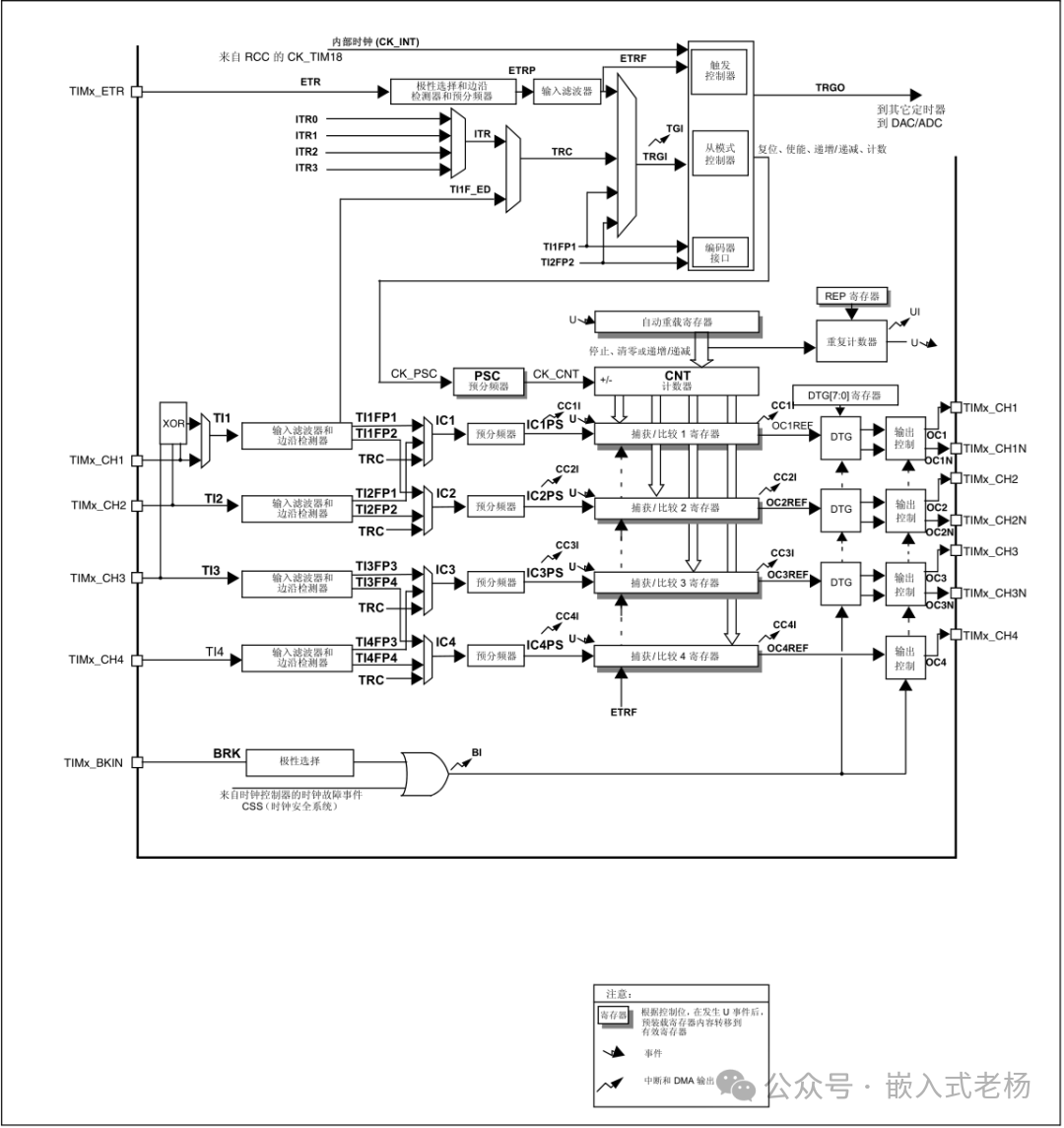
1.Clock Source Module
Internal Clock (CK_INT): Comes from the microcontroller’s RCC (Reset and Clock Control) module, which is the basic clock source for the timer, providing a stable clock signal for the timer’s counting operation. For example, with a default system clock of 84MHz, after appropriate prescaler configuration, it can provide a suitable frequency clock for the timer.
External Trigger Input (ETR): Can connect external signals through the TIMx_ETR pin, serving as the timer’s clock source or triggering the timer for counting operations. It can be a pulse signal used to implement external event-driven timing functions.
Internal Trigger Input (ITRx): Can select trigger signals from other timers (ITR0 – ITR3) as the current timer’s clock source or trigger source, facilitating synchronization or cascading operation between multiple timers.
2.Prescaler (PSC) Module
The prescaler is used to divide the input clock (CK_INT or ETR, etc.) to obtain the counter clock (CK_CNT). By configuring the prescaler value, the timer’s counting frequency can be adjusted. For example, if the prescaler value is set to 83, when the clock source frequency is 84MHz, the output clock frequency to the counter becomes 1MHz.
3.Counter (CNT) Module
The counter is the core part of the timer, performing counting operations based on the selected counting mode (up counting, down counting, center aligned counting, etc.). The counter’s count value is compared with the compare value, triggering corresponding events such as output compare, input capture, etc.
4.Input Capture Module (ICx, x = 1 – 4)
Input Filter and Edge Detector: Filters the signals input from the TIMx_CHx pin, removing noise interference and detecting the rising or falling edges of the signal.
Prescaler: Divides the filtered signal to adapt to different frequency input signals.
Capture/Compare Register (CCRx): Used to store the captured counter value, enabling measurement of parameters such as pulse width and frequency of the input signal. For example, when measuring encoder signals, the input capture function can obtain information about the encoder’s rotation direction and speed.
5.Output Compare Module (OCx, x = 1 – 4)
Capture/Compare Register (CCRx): Stores the compare value, which is compared with the counter’s value.
Output Control Logic: Controls the output state of the corresponding channel (TIMx_CHxN) based on the comparison result, achieving PWM output, level inversion, etc. By configuring output modes (e.g., PWM mode 1, PWM mode 2, etc.), different duty cycles and frequencies of PWM signals can be generated for applications such as motor control and LED dimming.
6.Brake (Break) Module
Inputs brake signals through the TIMx_BKIN pin. When a valid brake signal (polarity configurable) is detected, the timer output can be quickly stopped, placing the PWM output in a safe state (high level, low level, or high impedance), commonly used to protect circuits and prevent damage to power devices, such as quickly cutting off PWM output in case of overcurrent or overvoltage in motor control.
7.Dead Time Generation (DTG) Module
In complementary PWM outputs (e.g., for H-bridge circuits used in three-phase motor control), the dead time generation module inserts a brief delay during the switching of upper and lower bridge arms to ensure that both arms do not conduct simultaneously, avoiding short circuits. By configuring the dead time register, the length of the dead time can be adjusted.
8.Repeat Counter (REP) Module
The repeat counter is used to control the repeat cycle of the PWM signal. In advanced timers, it can achieve more flexible PWM output control. For example, in certain motor control algorithms, adjusting the repeat counter value can optimize the output characteristics of the PWM signal.
9.Trigger Controller Module
Used to generate trigger signals (TRGO), which can be output to other timers or trigger DAC/ADC and other peripherals for synchronous operations. It can also receive external trigger signals (TRGI) to control specific operations of the timer, such as starting the counter.
10.Slave Mode Controller Module
Used to configure the timer’s operation in slave mode, enabling functions such as reset, enable, increment/decrement counting, etc., allowing the timer to operate according to predetermined logic in conjunction with external trigger signals.
Operating Principles:
1.Clock Configuration and Counting
First, configure the appropriate clock source (internal clock or external trigger clock, etc.) through RCC. The clock signal is divided by the prescaler and drives the counter to count according to the selected counting mode. For example, in up counting mode, the counter starts from 0, and with each clock pulse, the count value increments until it reaches the preset auto-reload value (ARR), generating an overflow event.
2.Input Capture Workflow
When an external signal is input from the TIMx_CHx pin, it first passes through the input filter and edge detector, filtering out noise and detecting valid edges (rising edge, falling edge, or both edges). The signal is then divided according to the configured prescaler, and the current counter value is captured into the corresponding capture/compare register (CCRx). By recording the count values of two captures and the clock cycle, the frequency and pulse width of the input signal can be calculated.
3.Output Compare and PWM Generation
The counter’s value is continuously compared with the compare value in the capture/compare register (CCRx). Based on the comparison result, the output control logic controls the output state of the corresponding channel. In PWM mode, by adjusting the compare value and auto-reload value, the duty cycle and frequency of the PWM signal can be changed. For example, within one cycle, when the counter value is less than the compare value, one output level is produced; when the counter value is greater than or equal to the compare value, another output level is produced, thus generating a PWM waveform.
4.Brake and Dead Time Control
The brake pin (TIMx_BKIN) monitors the external brake signal. When the brake signal is valid, the timer output is forced into a safe state, stopping the PWM output. In complementary PWM output applications, the dead time generation module inserts specific delays during the switching of upper and lower bridge arms to ensure safe operation of the circuit.
5.Triggering and Synchronization
The trigger signal (TRGO) generated by the trigger controller can be used to synchronize other timers or peripherals, such as triggering the ADC for sampling. At the same time, the slave mode controller can receive external trigger signals (TRGI) to control the timer’s start, stop, and other operations, achieving coordinated operation between multiple timers and synchronization with external devices.

03
—
Function Description
1. Time Base Unit
The time base unit mainly consists of the prescaler (PSC), counter (CNT), and auto-reload register (ARR). Its function is to divide the input clock to generate the counting clock for the counter and set the counting period of the counter.
The timing diagram of the counter when the prescaler is divided from 1 to 2:
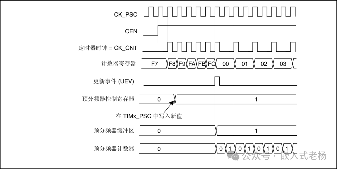
Note: When the timer time base unit operates, the initial prescaler control register value is 0, with a division factor of 1, CK_PSC and CK_CNT frequencies being the same. The counter increments from F7 to FC under CK_CNT drive, reaching the ARR value generates UEV and resets to 0. Afterward, writing a new value to TIMx_PSC makes the prescaler control register become 1. Due to the presence of the prescaler buffer, the division factor only changes to 2 after UEV occurs. At this point, the prescaler counter alternates between 0 and 1, halving the CK_CNT frequency, causing the counter to increment from 00 to 03 at a slower counting speed, taking more CK_PSC cycles.
2. Counter Modes
Incrementing Counting Mode: The counter starts from 0, incrementing by 1 on each rising edge of the counting clock. When the count value reaches the auto-reload value (ARR), an update event is generated, and the counter resets to zero, starting the counting process again. This is commonly used for simple timing functions, such as triggering an event at regular intervals.
Counter timing diagram, taking 2 divided internal clock as an example:
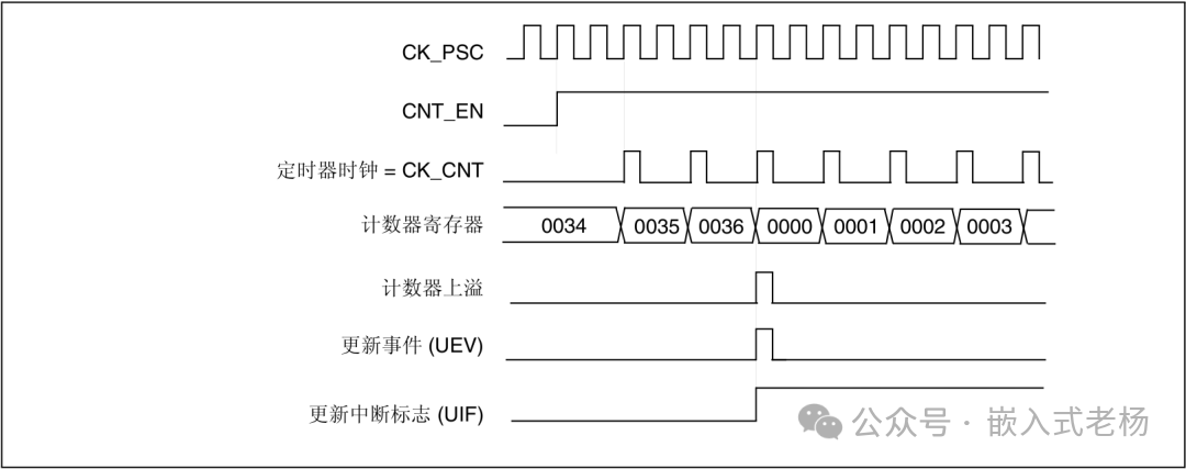
Note: In the timer incrementing counting mode, when CNT_EN is set to 1, activating the time base unit, the prescaler divides CK_PSC by 2 to generate CK_CNT (one CK_CNT valid edge is produced for every 2 CK_PSC pulses). The counter starts incrementing from the initial value 0034 under CK_CNT drive, sequentially changing to 0035, 0036. When the count value reaches the auto-reload value ARR (here 0036), an overflow occurs, triggering the update event UEV, and the counter automatically resets to 0000, starting a new incrementing cycle. The update interrupt flag UIF is also set, and if interrupts are enabled, it can trigger the timer update interrupt service routine, thus achieving the timing function in a loop.
Decrementing Counting Mode: The counter starts from the auto-reload value (ARR), decrementing by 1 on each rising edge of the counting clock. When the count value reaches 0, an update event is generated, and the counter reloads the ARR value, continuing to decrement. This can be used in countdown scenarios.
Counter timing diagram, taking 2 divided internal clock as an example:
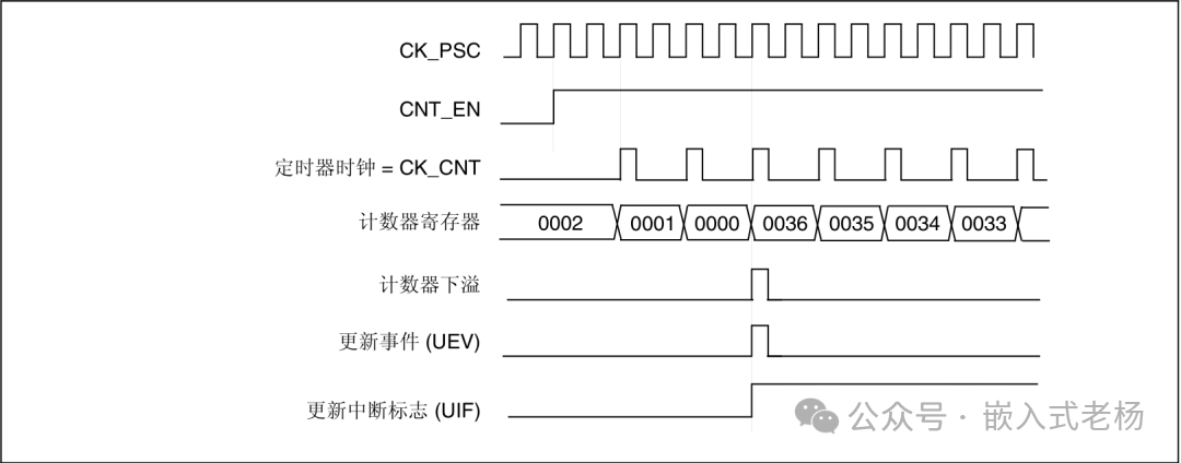
Note: In the decrementing counting mode, when CNT_EN is set to 1 to activate the time base unit, the prescaler divides CK_PSC by 2 to generate CK_CNT (one CK_CNT valid edge is produced for every 2 CK_PSC pulses). The counter starts from the initial value 0002, decrementing under CK_CNT drive to 0001, 0000. When the count value reaches 0000, an underflow occurs, triggering the update event UEV, and the counter automatically reloads to 0036, starting a new decrementing cycle (0036→0035→0034→…). The update interrupt flag UIF is also set, and if interrupts are enabled, it can trigger the timer update interrupt service routine, thus achieving the timing function in a loop.
Center Aligned Counting Mode: The counter starts incrementing from 0, and when it reaches half of the auto-reload value (ARR), it starts decrementing, going back to 0, and then incrementing again, repeating this cycle. This mode is commonly used to generate symmetrical PWM waveforms, suitable for SVPWM algorithms in motor control.
Counter timing diagram, taking 2 divided internal clock as an example:
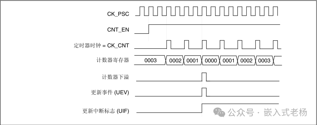
Note: In the center aligned mode, when CNT_EN is set to 1 to activate the time base unit, the prescaler divides CK_PSC by 2 to generate CK_CNT (one CK_CNT valid edge is produced for every 2 CK_PSC pulses). The counter first decrements from 0003, going through 0002, 0001 to 0000, producing an underflow, triggering the update event UEV. It then starts incrementing, changing sequentially to 0001, 0002, 0003, completing a “decrementing→underflow→incrementing” center aligned counting cycle. The update interrupt flag UIF is also set, and if interrupts are enabled, it can trigger the timer update interrupt service routine, thus achieving timing, reflecting the characteristics of the counter first decrementing and then incrementing in the center aligned mode.
3. Clock Selection
The clock sources for the advanced control timer have multiple options:
Internal Clock (CK_INT): Comes from the APB2 clock and is the most commonly used clock source, configured through RCC.
External Trigger Input (ETR): Introduces external signals through the TIMx_ETR pin as a clock source or trigger signal, capable of operating in external clock mode 2 for counting based on external events.
Internal Trigger Input (ITRx): Selects trigger signals from other timers (ITR0 – ITR3) as the current timer’s clock source or trigger source, achieving synchronization or cascading between timers.
4. Capture/Compare Functionality
The capture/compare functionality is mainly implemented through the capture/compare register (CCRx).
Input Capture Function:
The principle block diagram of channel 1 input capture is as follows:
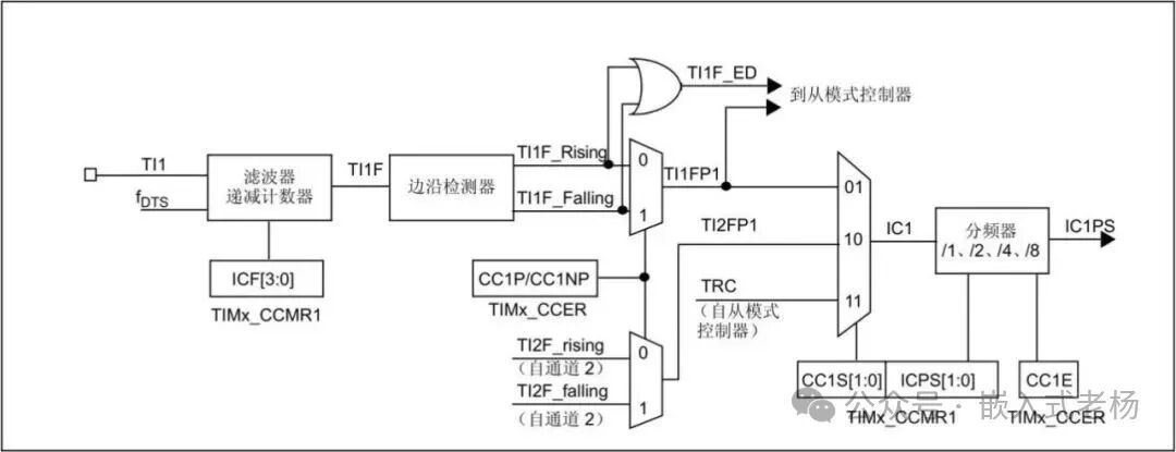
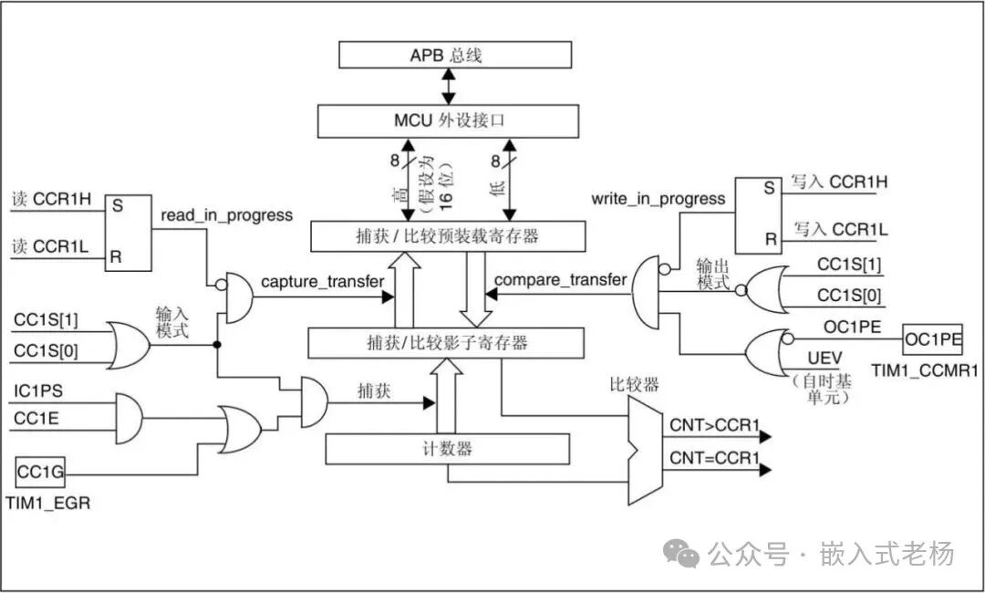
Note: In input capture mode, external signals are input through the TI1 pin, first filtered by the filter configured in TIMx_CCMR1 (including a decrementing counter, set by ICF [3:0]), and then processed by the edge detector (controlled by TIMx_CCER’s CC1P/CC1NP, etc., to detect rising/falling edges). The signal is then processed through a multiplexer (controlled by CC1S [1:0], which can select TI1FP1, TI2FP1, or TRC signals), followed by a divider (set by ICPS [1:0] for the division ratio). When the capture conditions are met (e.g., CC1E enabled), the counter value will be transferred to the capture/compare shadow register at the capture moment, then to the preload register, which can be read via the APB bus or MCU peripheral interface, enabling detection of input signal edges and capturing the corresponding counter values to measure frequency, pulse width, etc.
Output Compare Function:
The principle block diagram of channel 1 output compare is as follows:
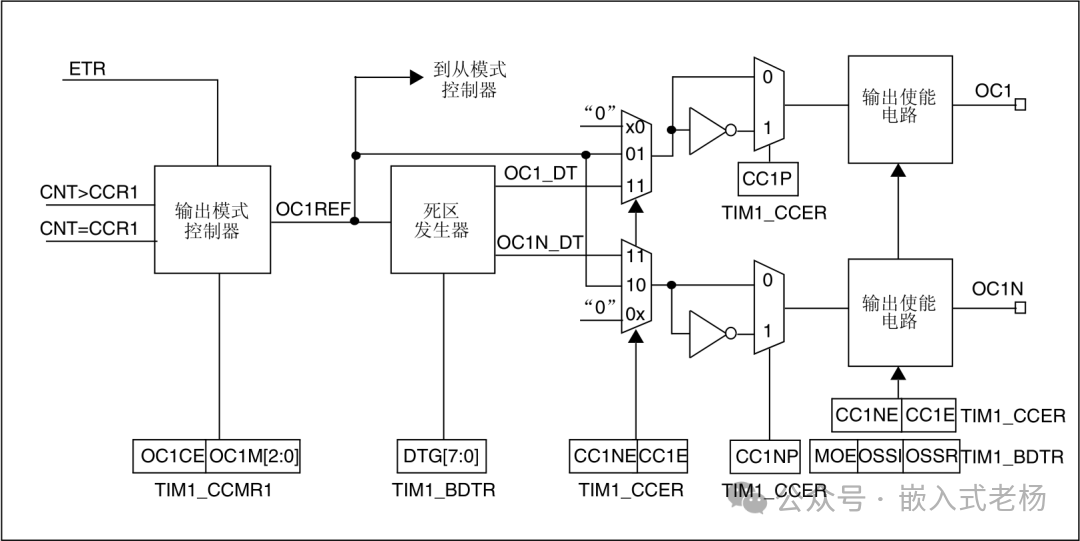
Note: In output compare mode, the counter (CNT) value is compared in real-time with the value in the capture/compare register (CCR1). The comparison result is sent to the output mode controller, which generates the reference signal OC1REF based on the configuration of OC1CE and OC1M [2:0] bits in the TIM1_CCMR1 register.
If complementary outputs are involved (used in scenarios requiring upper and lower bridge arm driving, such as motor control), the OC1REF signal will be transmitted to the dead time generator, which generates OC1_DT and OC1N_DT signals with dead time delays based on the dead time set in the TIM1_BDTR register, preventing both upper and lower bridge arms from conducting simultaneously. These signals are then processed through a multiplexer (controlled by CC1P, CC1NP, etc., in the TIM1_CCER register) and enter the output enable circuit, which determines whether to output the signal from the OC1 and OC1N pins based on the enable bits in the TIM1_CCER register (CC1E, CC1NE, etc.) and the configuration in the TIM1_BDTR register (MOE, OSS, OSSR, etc.), thus controlling external devices such as motor speed and direction, LED brightness, etc.
5. PWM Input Mode:
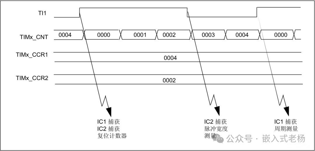
In PWM input mode, the TI1 pin receives the PWM signal. When the signal edge arrives, it triggers IC1 and IC2 capture operations, resetting the counter (TIMx_CNT to 0000) at the first edge, while TIMx_CCR1 and TIMx_CCR2 record the counter value at that moment. Subsequent signal falling edges trigger IC2 capture, and the difference between TIMx_CCR2 and TIMx_CCR1 can measure pulse width. The next rising edge triggers IC1 capture, and combining the previous and current values of TIMx_CCR1 (e.g., from 0004 to 0000) can complete period measurement, thus achieving precise detection of the input PWM signal’s pulse width and period.
6. PWM Output Mode
Taking the edge-aligned mode PWM waveform (ARR=8) as an example:
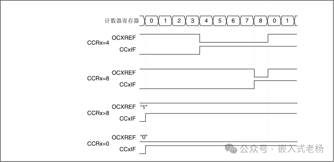
Note: In edge-aligned mode, the counter increments with the clock (e.g., cycling from 0 to 8), and the output compare reference signal OCXREF and flag CCxIF status are determined by the relationship between the capture/compare register CCRx and the counter value: when CCRx=4, the counter reaching 4 causes OCXREF to toggle, setting CCxIF; when CCRx=8, reaching 8 triggers OCXREF to toggle, setting CCxIF; when CCRx>8, OCXREF remains “1”, and when the counter reaches 0, CCxIF is set; when CCRx=0, OCXREF remains “0”, and when the counter reaches 0, CCxIF is set. Through this logic of counter incrementing and comparing with CCRx, edge-aligned PWM waveforms are generated, achieving the function of outputting different duty cycle signals as configured.
Taking the center-aligned mode PWM waveform (ARR=8) as an example:
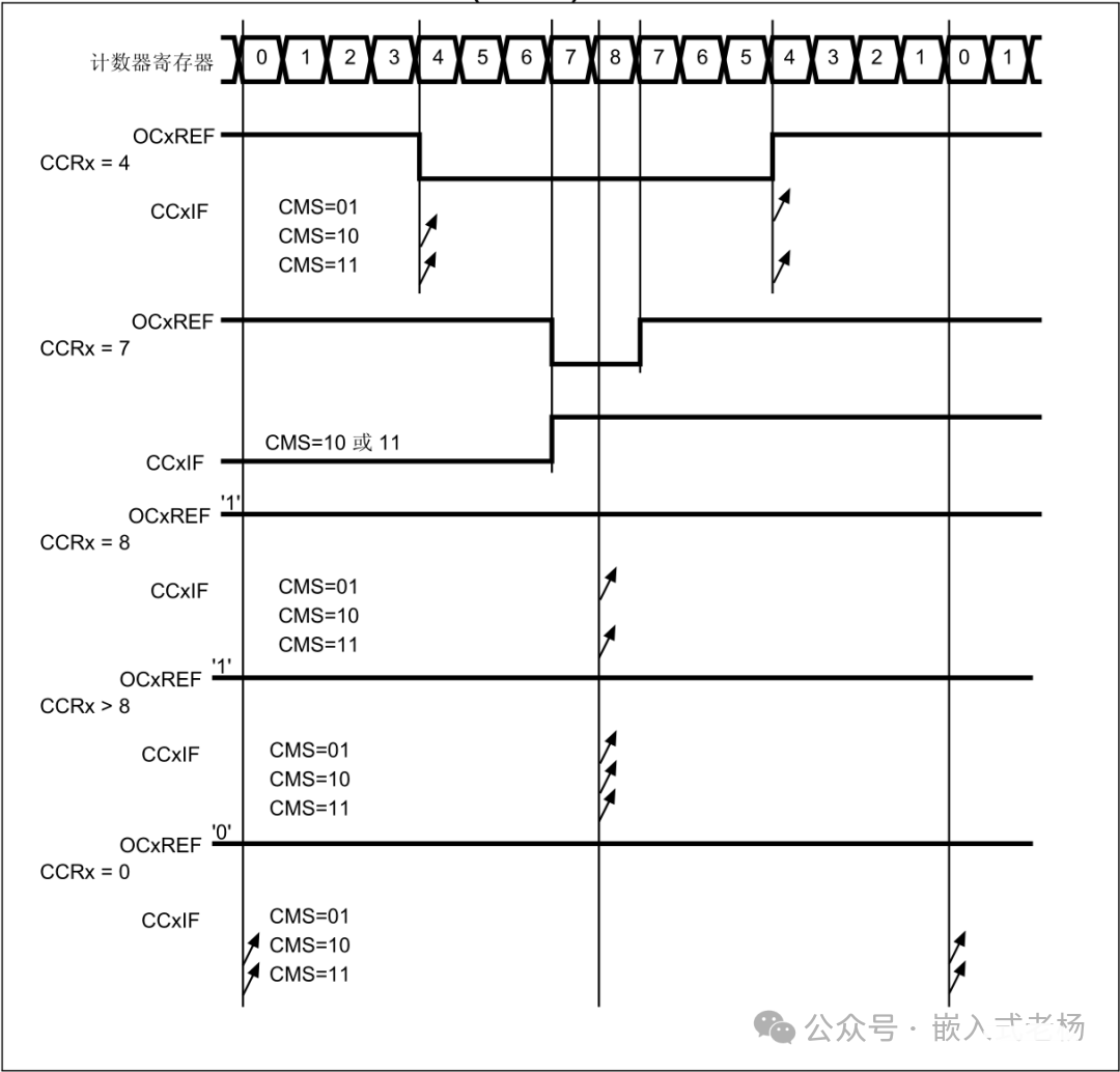
Note: In PWM output mode – center-aligned mode, the counter first increments from 0 to the maximum value (e.g., 8), then decrements back to 0, repeating this cycle. The output compare reference signal OCxREF state depends on the comparison result between the capture/compare register CCRx and the counter value, with the flag CCxIF set under specific conditions. When CCRx = 4, the counter incrementing or decrementing through 4 causes OCxREF to toggle, and different center-aligned mode selection bits (CMS = 01, 10, 11) determine the timing of CCxIF being set; when CCRx = 7, the counter incrementing or decrementing through 7 causes OCxREF to toggle, with CCxIF set in CMS = 10 or 11; when CCRx = 8, the counter incrementing or decrementing through 8 causes OCxREF state to change, with CCxIF set based on CMS; when CCRx > 8, OCxREF remains high, and CCxIF is set when the counter passes the CCRx value, based on CMS; when CCRx = 0, OCxREF remains low, and CCxIF is set when the counter passes 0, based on CMS. Through this mechanism of bidirectional counting of the counter and comparison with CCRx, symmetrical PWM waveforms are generated.
7. Forced Output Mode
In forced output mode, by configuring related registers (e.g., TIMx_CCMR1, TIMx_CCER, etc.), the conventional comparison mechanism between the counter and capture/compare register (CCRx) can be bypassed, directly forcing the output channel (OCx) to output a specified level (high level, low level, or toggle level as needed). Regardless of the current counter value or the counting mode of the counter and the value of CCRx, as long as the forced output mode is enabled, the output channel’s level state can be immediately changed according to the settings, commonly used for quick and direct control of output states.
8. One Pulse Mode
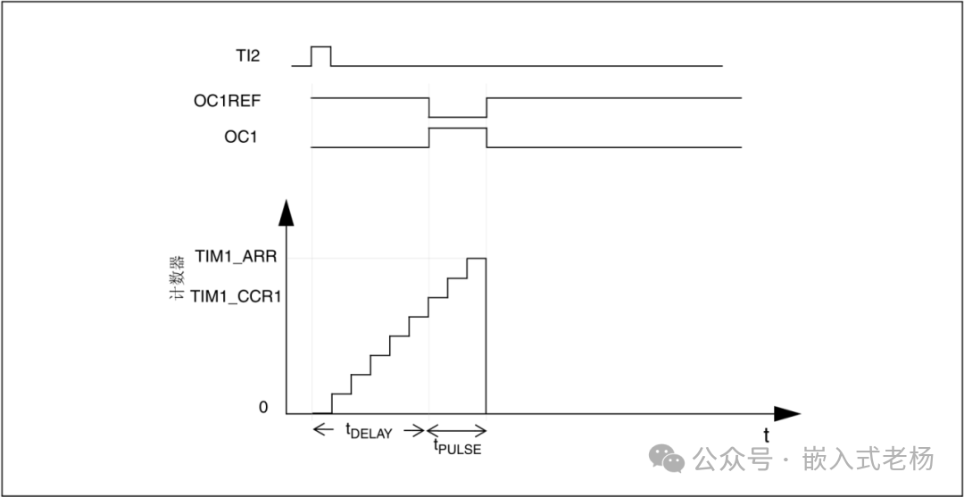
Note: In one pulse mode, the TI2 pin inputs the trigger signal. After triggering, the timer counter starts incrementing, and after a delay of t_DELAY (determined by the relationship between TIM1_CCR1 and the counter), the OC1REF signal toggles. After a pulse width of t_PULSE (determined by the difference between TIM1_ARR and TIM1_CCR1), the OC1REF signal toggles back to its original state, and OC1 output changes with OC1REF, thus outputting a single pulse with specific delay and width.
9. Encoder Interface Mode
The relationship between counting direction and encoder signals:
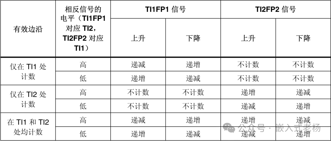
Configuration as follows:
-
CC1S=”01″ (TIMx_CCMR1 register, TI1FP1 mapped to TI1).
-
CC2S=”01″ (TIMx_CCMR2 register, TI1FP2 mapped to TI2).
-
CC1P=”0″, CC1NP=”0″, and IC1F =”0000″ (TIMx_CCER register, TI1FP1 not inverted, TI1FP1=TI1).
-
CC2P=”0″, CC2NP=”0″, and IC2F =”0000″ (TIMx_CCER register, TI1FP2 not inverted, TI1FP2=TI2).
-
SMS=”011″ (TIMx_SMCR register, both inputs are valid on rising and falling edges).
-
CEN=”1″ (TIMx_CR1 register, enabling the counter).
Example of counter operation in encoder interface mode:
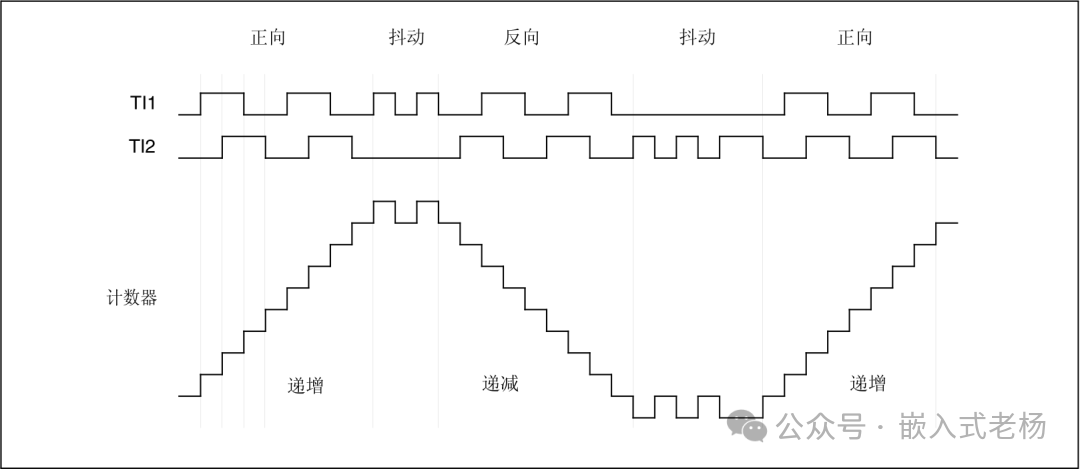
The behavior of the counter when TI1FP1 is inverted (other configurations are the same as above).
Example of encoder interface mode with TI1FP1 inverted:
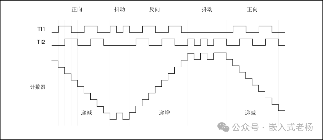
Note: In encoder interface mode, TI1 and TI2 input the encoder quadrature signals. After configuration (CC1S, CC2S set to “01” to map signals, CCxP, CCxNP, etc., set to non-inverted, SMS set to “011” to make both inputs valid on edges, CEN to enable the counter), the counter increments in the forward direction and decrements in the reverse direction based on the edges and level combinations of TI1FP1 (i.e., TI1) and TI2FP2 (i.e., TI2) signals (refer to the table rules). In case of jitter, signal changes will also trigger counting adjustments, thus tracking the encoder’s rotation direction and displacement in real-time, achieving detection of the encoder’s motion state.

04
—
Program Design Example
The above is the configuration process for the input capture function, output compare function, PWM input mode, PWM output mode (taking edge-aligned mode PWM waveform (ARR=8) as an example), PWM output mode (taking center-aligned mode PWM waveform (ARR=8) as an example), forced output mode, one pulse mode, and encoder interface mode of the STM32F4xx advanced control timer. In all modes, the prescaler divides CK_PSC by 2.
main.c
#include "main.h"
#include "timer_config.h"
/* Function declarations */
void SystemClock_Config(void);
static void MX_GPIO_Init(void);
int main(void) {
    HAL_Init();
    SystemClock_Config();
    MX_GPIO_Init();
    /* Initialize the desired timer mode */
    // TIM_InputCapture_Init();
    // TIM_OutputCompare_Init();
    // TIM_PWMInput_Init();
    // TIM_PWMOutput_EdgeAligned_Init();
    // TIM_PWMOutput_CenterAligned_Init();
    // TIM_ForceOutput_Init();
    // TIM_OnePulse_Init();
    // TIM_EncoderInterface_Init();
    while (1) {
        /* Main loop code */
    }
}
timer_config.c
#include "timer_config.h"
/* Timer handle definitions */
TIM_HandleTypeDef htim1;
TIM_HandleTypeDef htim2;
TIM_HandleTypeDef htim3;
TIM_HandleTypeDef htim4;
/* Input capture mode configuration */
void TIM_InputCapture_Init(void) {
    TIM_IC_InitTypeDef sConfigIC = {0};
    /* Enable timer clock */
    __HAL_RCC_TIM1_CLK_ENABLE();
    /* Timer basic configuration */
    htim1.Instance = TIM1;
    htim1.Init.Prescaler = 1;              /* 2 division (PSC=1) */
    htim1.Init.CounterMode = TIM_COUNTERMODE_UP;
    htim1.Init.Period = 0xFFFF;
    htim1.Init.ClockDivision = TIM_CLOCKDIVISION_DIV1;
    htim1.Init.RepetitionCounter = 0;
    if (HAL_TIM_IC_Init(&htim1) != HAL_OK) {
        Error_Handler();
    }
    /* Input capture channel configuration */
    sConfigIC.ICPolarity = TIM_INPUTCHANNELPOLARITY_RISING;
    sConfigIC.ICSelection = TIM_ICSELECTION_DIRECTTI;
    sConfigIC.ICPrescaler = TIM_ICPSC_DIV1;
    sConfigIC.ICFilter = 0;
    if (HAL_TIM_IC_ConfigChannel(&htim1, &sConfigIC, TIM_CHANNEL_1) != HAL_OK) {
        Error_Handler();
    }
    /* Start input capture */
    HAL_TIM_IC_Start_IT(&htim1, TIM_CHANNEL_1);
}
/* Output compare mode configuration */
void TIM_OutputCompare_Init(void) {
    TIM_OC_InitTypeDef sConfigOC = {0};
    /* Enable timer clock */
    __HAL_RCC_TIM2_CLK_ENABLE();
    /* Timer basic configuration */
    htim2.Instance = TIM2;
    htim2.Init.Prescaler = 1;              /* 2 division (PSC=1) */
    htim2.Init.CounterMode = TIM_COUNTERMODE_UP;
    htim2.Init.Period = 1000;
    htim2.Init.ClockDivision = TIM_CLOCKDIVISION_DIV1;
    if (HAL_TIM_OC_Init(&htim2) != HAL_OK) {
        Error_Handler();
    }
    /* Output compare channel configuration */
    sConfigOC.OCMode = TIM_OCMODE_TOGGLE;
    sConfigOC.Pulse = 500;
    sConfigOC.OCPolarity = TIM_OCPOLARITY_HIGH;
    sConfigOC.OCFastMode = TIM_OCFAST_DISABLE;
    if (HAL_TIM_OC_ConfigChannel(&htim2, &sConfigOC, TIM_CHANNEL_1) != HAL_OK) {
        Error_Handler();
    }
    /* Start output compare */
    HAL_TIM_OC_Start(&htim2, TIM_CHANNEL_1);
}
/* PWM input mode configuration */
void TIM_PWMInput_Init(void) {
    TIM_IC_InitTypeDef sConfigIC = {0};
    /* Enable timer clock */
    __HAL_RCC_TIM3_CLK_ENABLE();
    /* Timer basic configuration */
    htim3.Instance = TIM3;
    htim3.Init.Prescaler = 1;              /* 2 division (PSC=1) */
    htim3.Init.CounterMode = TIM_COUNTERMODE_UP;
    htim3.Init.Period = 0xFFFF;
    htim3.Init.ClockDivision = TIM_CLOCKDIVISION_DIV1;
    if (HAL_TIM_IC_Init(&htim3) != HAL_OK) {
        Error_Handler();
    }
    /* Input capture channel configuration (PWM input mode) */
    sConfigIC.ICPolarity = TIM_INPUTCHANNELPOLARITY_RISING;
    sConfigIC.ICSelection = TIM_ICSELECTION_DIRECTTI;
    sConfigIC.ICPrescaler = TIM_ICPSC_DIV1;
    sConfigIC.ICFilter = 0;
    if (HAL_TIM_IC_ConfigChannel(&htim3, &sConfigIC, TIM_CHANNEL_1) != HAL_OK) {
        Error_Handler();
    }
    sConfigIC.ICPolarity = TIM_INPUTCHANNELPOLARITY_FALLING;
    sConfigIC.ICSelection = TIM_ICSELECTION_INDIRECTTI;
    if (HAL_TIM_IC_ConfigChannel(&htim3, &sConfigIC, TIM_CHANNEL_2) != HAL_OK) {
        Error_Handler();
    }
    /* Start PWM input capture */
    HAL_TIM_IC_Start(&htim3, TIM_CHANNEL_1);
    HAL_TIM_IC_Start(&htim3, TIM_CHANNEL_2);
}
/* PWM output mode - edge-aligned configuration */
void TIM_PWMOutput_EdgeAligned_Init(void) {
    TIM_OC_InitTypeDef sConfigOC = {0};
    /* Enable timer clock */
    __HAL_RCC_TIM1_CLK_ENABLE();
    /* Timer basic configuration */
    htim1.Instance = TIM1;
    htim1.Init.Prescaler = 1;              /* 2 division (PSC=1) */
    htim1.Init.CounterMode = TIM_COUNTERMODE_UP;
    htim1.Init.Period = 8;                 /* ARR=8 */
    htim1.Init.ClockDivision = TIM_CLOCKDIVISION_DIV1;
    htim1.Init.RepetitionCounter = 0;
    if (HAL_TIM_PWM_Init(&htim1) != HAL_OK) {
        Error_Handler();
    }
    /* PWM output channel configuration */
    sConfigOC.OCMode = TIM_OCMODE_PWM1;
    sConfigOC.Pulse = 4;                   /* 50% duty cycle */
    sConfigOC.OCPolarity = TIM_OCPOLARITY_HIGH;
    sConfigOC.OCNPolarity = TIM_OCNPOLARITY_HIGH;
    sConfigOC.OCFastMode = TIM_OCFAST_DISABLE;
    sConfigOC.OCIdleState = TIM_OCIDLESTATE_RESET;
    sConfigOC.OCNIdleState = TIM_OCNIDLESTATE_RESET;
    if (HAL_TIM_PWM_ConfigChannel(&htim1, &sConfigOC, TIM_CHANNEL_1) != HAL_OK) {
        Error_Handler();
    }
    /* Start PWM output */
    HAL_TIM_PWM_Start(&htim1, TIM_CHANNEL_1);
}
/* PWM output mode - center-aligned configuration */
void TIM_PWMOutput_CenterAligned_Init(void) {
    TIM_OC_InitTypeDef sConfigOC = {0};
    /* Enable timer clock */
    __HAL_RCC_TIM1_CLK_ENABLE();
    /* Timer basic configuration */
    htim1.Instance = TIM1;
    htim1.Init.Prescaler = 1;              /* 2 division (PSC=1) */
    htim1.Init.CounterMode = TIM_COUNTERMODE_CENTERALIGNED1; /* Center aligned mode 1 */
    htim1.Init.Period = 8;                 /* ARR=8 */
    htim1.Init.ClockDivision = TIM_CLOCKDIVISION_DIV1;
    htim1.Init.RepetitionCounter = 0;
    if (HAL_TIM_PWM_Init(&htim1) != HAL_OK) {
        Error_Handler();
    }
    /* PWM output channel configuration */
    sConfigOC.OCMode = TIM_OCMODE_PWM1;
    sConfigOC.Pulse = 4;                   /* 50% duty cycle */
    sConfigOC.OCPolarity = TIM_OCPOLARITY_HIGH;
    sConfigOC.OCNPolarity = TIM_OCNPOLARITY_HIGH;
    sConfigOC.OCFastMode = TIM_OCFAST_DISABLE;
    sConfigOC.OCIdleState = TIM_OCIDLESTATE_RESET;
    sConfigOC.OCNIdleState = TIM_OCNIDLESTATE_RESET;
    if (HAL_TIM_PWM_ConfigChannel(&htim1, &sConfigOC, TIM_CHANNEL_1) != HAL_OK) {
        Error_Handler();
    }
    /* Start PWM output */
    HAL_TIM_PWM_Start(&htim1, TIM_CHANNEL_1);
}
/* Forced output mode configuration */
void TIM_ForceOutput_Init(void) {
    TIM_OC_InitTypeDef sConfigOC = {0};
    /* Enable timer clock */
    __HAL_RCC_TIM2_CLK_ENABLE();
    /* Timer basic configuration */
    htim2.Instance = TIM2;
    htim2.Init.Prescaler = 1;              /* 2 division (PSC=1) */
    htim2.Init.CounterMode = TIM_COUNTERMODE_UP;
    htim2.Init.Period = 1000;
    htim2.Init.ClockDivision = TIM_CLOCKDIVISION_DIV1;
    if (HAL_TIM_OC_Init(&htim2) != HAL_OK) {
        Error_Handler();
    }
    /* Forced output channel configuration */
    sConfigOC.OCMode = TIM_OCMODE_FORCED_ACTIVE; /* Forced output high level */
    sConfigOC.OCPolarity = TIM_OCPOLARITY_HIGH;
    if (HAL_TIM_OC_ConfigChannel(&htim2, &sConfigOC, TIM_CHANNEL_1) != HAL_OK) {
        Error_Handler();
    }
    /* Start timer */
    HAL_TIM_OC_Start(&htim2, TIM_CHANNEL_1);
}
/* One pulse mode configuration */
void TIM_OnePulse_Init(void) {
    TIM_OC_InitTypeDef sConfigOC = {0};
    /* Enable timer clock */
    __HAL_RCC_TIM3_CLK_ENABLE();
    /* Timer basic configuration */
    htim3.Instance = TIM3;
    htim3.Init.Prescaler = 1;              /* 2 division (PSC=1) */
    htim3.Init.CounterMode = TIM_COUNTERMODE_UP;
    htim3.Init.Period = 1000;
    htim3.Init.ClockDivision = TIM_CLOCKDIVISION_DIV1;
    if (HAL_TIM_OnePulse_Init(&htim3, TIM_OPMODE_SINGLE, TIM_OUTPUTSTATE_ENABLE, TIM_OUTPUTSTATE_DISABLE) != HAL_OK) {
        Error_Handler();
    }
    /* One pulse channel configuration */
    sConfigOC.OCMode = TIM_OCMODE_PWM1;
    sConfigOC.Pulse = 500;                 /* Pulse width */
    sConfigOC.OCPolarity = TIM_OCPOLARITY_HIGH;
    sConfigOC.OCFastMode = TIM_OCFAST_DISABLE;
    if (HAL_TIM_OC_ConfigChannel(&htim3, &sConfigOC, TIM_CHANNEL_1) != HAL_OK) {
        Error_Handler();
    }
}
/* Encoder interface mode configuration */
void TIM_EncoderInterface_Init(void) {
    TIM_Encoder_InitTypeDef sConfig = {0};
    /* Enable timer clock */
    __HAL_RCC_TIM4_CLK_ENABLE();
    /* Encoder interface configuration */
    htim4.Instance = TIM4;
    htim4.Init.Prescaler = 1;              /* 2 division (PSC=1) */
    htim4.Init.CounterMode = TIM_COUNTERMODE_UP;
    htim4.Init.Period = 65535;             /* Maximum counting range */
    htim4.Init.ClockDivision = TIM_CLOCKDIVISION_DIV1;
    sConfig.EncoderMode = TIM_ENCODERMODE_TI12;
    sConfig.IC1Polarity = TIM_ICPOLARITY_RISING;
    sConfig.IC1Selection = TIM_ICSELECTION_DIRECTTI;
    sConfig.IC1Prescaler = TIM_ICPSC_DIV1;
    sConfig.IC1Filter = 0;
    sConfig.IC2Polarity = TIM_ICPOLARITY_RISING;
    sConfig.IC2Selection = TIM_ICSELECTION_DIRECTTI;
    sConfig.IC2Prescaler = TIM_ICPSC_DIV1;
    sConfig.IC2Filter = 0;
    if (HAL_TIM_Encoder_Init(&htim4, &sConfig) != HAL_OK) {
        Error_Handler();
    }
    /* Start encoder interface */
    HAL_TIM_Encoder_Start(&htim4, TIM_CHANNEL_1 | TIM_CHANNEL_2);
}
 This article’s case uses the following hardware and software:
1. Microcontroller model: STM32F407ZGT6 (25MHz external crystal);
2. Software development environment: Keil MDK v5.36;
3. Pack version: STM32F4xx_DFP v3.0.0;
4. Compiler: ARM Compiler v5;
5. STM32 project version: Standard HAL library or register version;
6. Downloader: JLINK downloader, SWD interface;
7. This software and hardware case is for personal learning only and must not be used for commercial purposes.
References for this article:
“STM32F4xx Chinese Reference Manual (RM0090)”;
“STM32F405xx STM32F407xx Datasheet (DS8626)”.