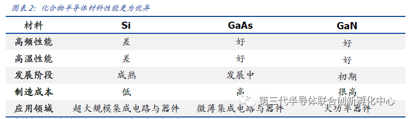
Compound semiconductors have excellent performance and a broad development prospect. Compound semiconductors mainly refer to second and third generation semiconductors such as Gallium Arsenide (GaAs), Gallium Nitride (GaN), and Silicon Carbide (SiC). Compared to the first generation of elemental semiconductors, they are significantly superior in high-frequency and high-temperature performance.
-
Gallium Arsenide: It features high frequency, radiation resistance, and high-temperature tolerance, making it widely used in wireless communication. It has become the mainstream material for PA and Switch.
-
Gallium Nitride: It is mainly applied in communication base stations and power devices, offering high amplifier efficiency and high power density, thus saving a lot of electrical energy while reducing the size and weight of base stations.
-
Silicon Carbide: It is primarily used in high-power high-frequency power devices. IHS predicts that by 2025, the market size for SiC power semiconductors is expected to reach $3 billion. In the next decade, SiC devices will begin to be widely applied in industrial and electric vehicle fields. Recently, the industrialization progress of silicon carbide has accelerated, with midstream manufacturers like STMicroelectronics and Infineon starting to secure upstream wafer sources.
What Are Compound Semiconductors?
Semi-conductor materials can be divided into two categories: elemental semiconductors and compound semiconductors. The former includes semiconductors formed from elements like Silicon (Si) and Germanium (Ge), while the latter includes compounds like Gallium Arsenide (GaAs), Gallium Nitride (GaN), and Silicon Carbide (SiC).Semiconductors have mainly undergone three generations of changes in the past.Gallium Arsenide (GaAs), Gallium Nitride (GaN), and Silicon Carbide (SiC) semiconductors respectively represent the second and third generations and are significantly superior to the first generation in high-frequency and high-temperature performance, though they come with higher manufacturing costs, making them the new aristocrats of semiconductors.
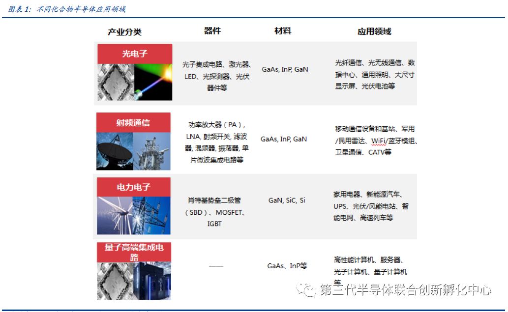
Among the three major compound semiconductor materials, GaAs accounts for a large share, mainly used in the communications field, with a global market capacity approaching $10 billion, benefiting mainly from upgrades in communication RF chips, especially PA; GaN has superior high-power and high-frequency performance, mainly applied in military fields, with a current market capacity of less than $1 billion, but is expected to see widespread application as costs decrease; SiC is primarily used as a high-power semiconductor material in automotive and industrial power electronics, having huge advantages in high-power conversion applications.
Beyond Moore: Continuous Development of Optical, RF, Power, and Other Analog ICs
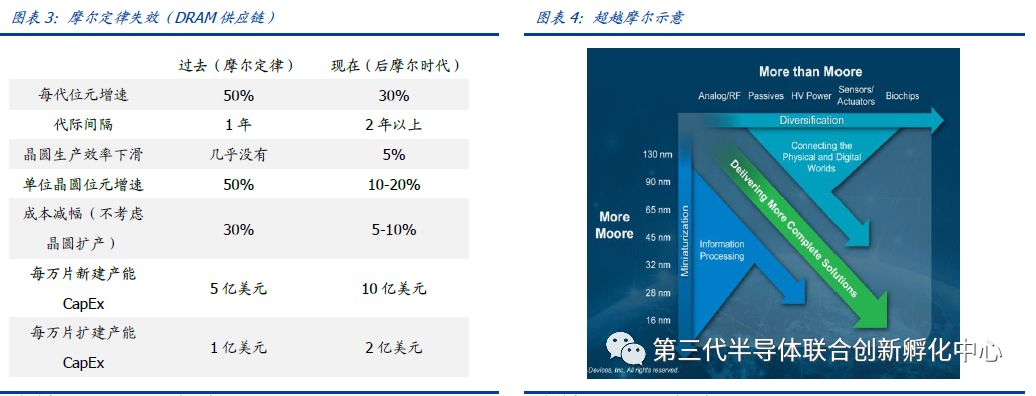
Moore’s Law is slowing down, leading to a differentiation in integrated circuit development. Currently, the development of integrated circuits mainly follows two directions: More Moore (Deep Moore) and More than Moore (Beyond Moore). Moore’s Law states that the number of transistors will double in the same area approximately every 18 months, while the price halves. However, it encountered obstacles at 28nm, where although the number of transistors doubled, the price did not decrease by half. More Moore (Deep Moore) refers to continuing to improve process node technology and entering the post-Moore era. Meanwhile, More than Moore (Beyond Moore) has been proposed, focusing on achieving more applications by adding more functions to single-chip ICs.
Analog ICs are more suited to the More than Moore (Beyond Moore) approach. Advanced processes and high integration can provide better performance and lower costs for digital ICs, but this is not applicable to analog ICs. Analog circuits like RF circuits often require large inductors, and advanced process integration has minimal impact while increasing costs; Advanced processes are often used in low-power environments, but RF, power, and other analog ICs operate in high-frequency, high-power fields, and advanced processes can even have a negative impact on performance; The linearity of analog circuits at low power and voltage is also hard to guarantee. The main technology for PA is GaAs, while the main technology for switches is SOI. The More than Moore (Beyond Moore) approach can achieve a combination of different technologies and processes, providing a pathway for the further development of analog ICs.
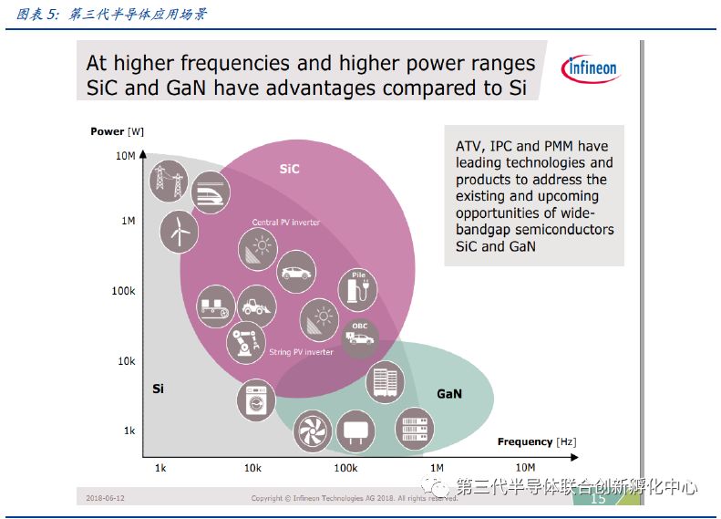
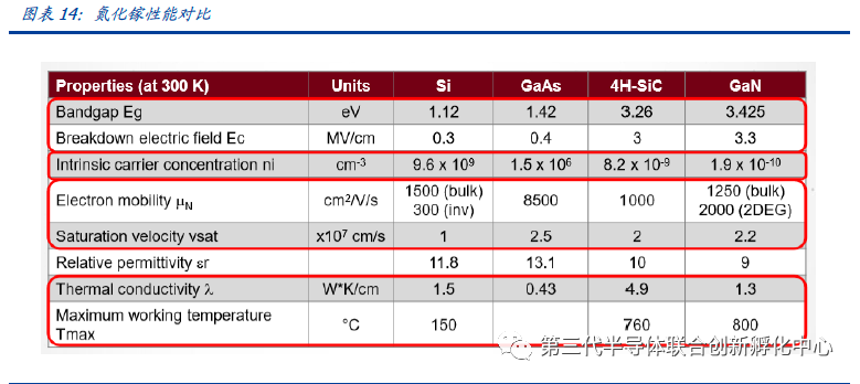
Third-generation semiconductors adapt to more application scenarios. Silicon-based semiconductors have characteristics such as high-temperature resistance, good radiation resistance, ease of manufacturing, and high stability. With over 99% of integrated circuits made from silicon, it is widely used. However, silicon-based semiconductors are not suitable for high-frequency, high-power applications. In the 2G, 3G, and 4G eras, the main material for PA was GaAs, but in the 5G era, the main material is GaN. The frequency of 5G is higher, and its jumpy reflection characteristics lead to shorter transmission distances. Since millimeter waves require very high power, GaN, with its small size and high power, is currently the most suitable PA material for the 5G era. Third-generation semiconductors like SiC and GaN will better meet future application needs.
Analog ICs focus on voltage and current control, distortion rate, power consumption, reliability, and stability. Designers need to consider the impact of various components on the performance of analog circuits, making the design difficult. Digital circuits pursue computational speed and cost, often using CMOS technology, and have developed along Moore’s Law for many years, continuously adopting more efficient algorithms to process digital signals or using new processes to improve integration and reduce costs. However, excessively high process node technology is often detrimental to achieving low distortion and high signal-to-noise ratio in analog ICs or meeting the requirements for high voltage or large current output to drive other components, thus analog ICs have lower demands for node evolution compared to digital ICs. The lifecycle of analog chips is also longer, generally lasting 10 years or more. For example, the operational amplifier μA741 launched by Fairchild in 1968 has been sold for nearly fifty years and still has customers using it.
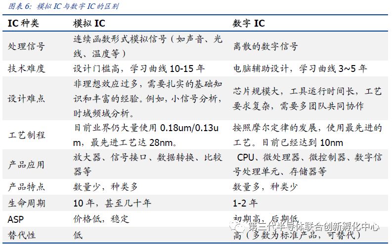
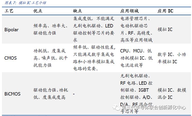
Currently, digital ICs mostly use CMOS technology, while analog ICs use a variety of processes and are not bound by Moore’s Law. The manufacturing processes for analog ICs include Bipolar process, CMOS process, and BiCMOS process. In high-frequency fields, SiGe technology, GaAs technology, and SOI technology can also be combined with Bipolar and BiCMOS processes to achieve better performance. In the power field, SOI technology and BCD (integrating DMOS and other power devices based on BiCMOS) technology also perform better. Analog ICs have a wide range of applications, and the usage scenarios vary, so the manufacturing processes will also change accordingly.
Gallium Arsenide (GaAs): Core Material for Wireless Communication, Benefiting from the 5G Trend
Compared to the first generation of silicon semiconductors, Gallium Arsenide has high frequency, radiation resistance, and high-temperature tolerance, making it widely used in mainstream commercial wireless communication, optical communication, and defense military applications. The popularity of wireless communication, combined with the limitations of silicon in high-frequency characteristics, has led to the emergence of Gallium Arsenide materials, which are widely used in the wireless communication field.
The baseband and RF modules are the core components that complete the 3/4/5G cellular communication functions. The RF module generally consists of transceivers and frontend modules (PA, Switch, Filter). Among them, Gallium Arsenide has become the mainstream material for PA and Switch.
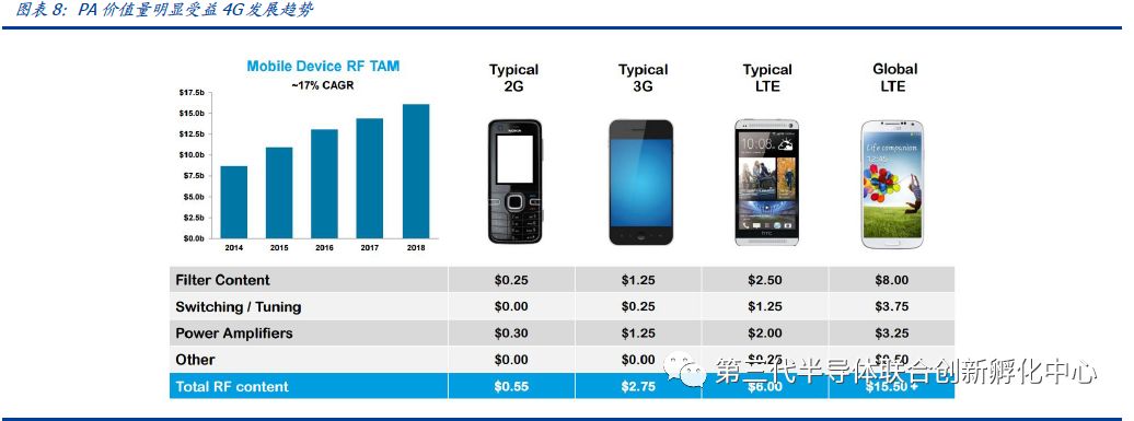
The continuous increase in 4G/5G frequency bands drives the growth of PA usage. Since a single PA chip can only handle signals in a fixed frequency band, the increase in cellular communication frequency bands significantly boosts the PA consumption of smartphones. With the popularity of 4G communication, the frequency bands for mobile communication expanded rapidly from 6 in 2010 to 43, and in the 5G era, it is expected to exceed 60. Currently, mainstream 4G communication uses 5 frequency bands and 13 modes, averaging 7 PAs and 4 RF switches per device.
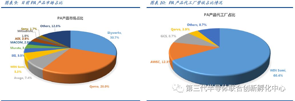
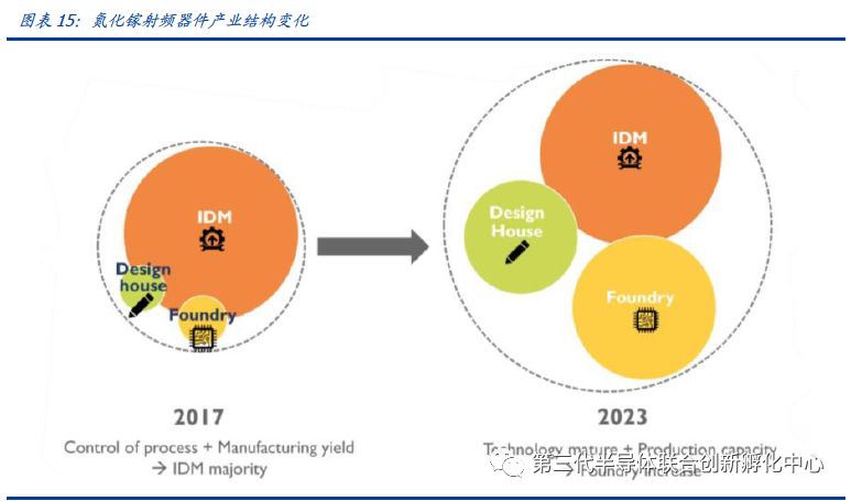
Currently, leading companies in Gallium Arsenide still primarily operate under the IDM model, including US companies Skyworks, Qorvo, Broadcom/Avago, Cree, and Germany’s Infineon. Meanwhile, we also notice that the industry development model is gradually shifting from the IDM model to design + foundry production, with a typical event being the continuous increase in foundry ratios, such as Avago selling its Colorado plant to Win Semiconductors last year. We believe that the technology for GaAs substrates and devices is continuously maturing and standardizing, with significant value in product diversification and device design, leading to an increase in the division of design + manufacturing models.
According to estimates from third-party research institutions like Yole Development, the global market size for GaAs devices used in PAs reached $8-9 billion in 2017, with most market share concentrated in the three giants: Skyworks, Qorvo, and Avago. It is expected that with communication upgrades, the market will officially exceed $10 billion in the next two years.
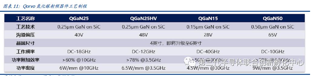
At the same time, the application market does not require advanced process technology below 60 nm linewidth, and not pursuing the most advanced process technology is another characteristic. Compound semiconductors are directed towards RF, high voltage, high power, optoelectronics, etc., without needing advanced processes. GaAs and GaN devices primarily use processes above 0.13 and 0.18μm. Qorvo is currently developing a 90nm process. Additionally, due to the size limitations of GaAs and SiC substrates, current production lines are mostly 4-inch and 6-inch. For example, Qorvo’s GaN process generally has linewidths between 0.25-0.50μm, with 4-inch production lines being predominant.
Gallium Nitride & Silicon Carbide: Significant Advantages in High Voltage and High Frequency
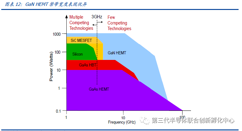
Gallium Nitride (GaN) and Silicon Carbide (SiC) are known as the dual heroes of third-generation semiconductor materials. Due to their different performances, their application fields also vary. Gallium Nitride has advantages such as a wide bandgap, high breakdown electric field, high saturation electron velocity, high thermal conductivity, stable chemical properties, and strong radiation resistance, making it one of the preferred materials for high-temperature, high-frequency, and high-power microwave devices.
▌Gallium Nitride: The Arrival of 5G Era, Broad Prospects for RF Applications
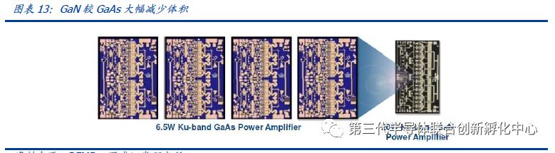
Currently, two-thirds of Gallium Nitride devices are used in military electronics, such as military communications, electronic interference, and radar; In the civilian sector, Gallium Nitride is mainly applied in communication base stations and power devices. The amplifier efficiency of Gallium Nitride base station PAs is higher than that of other materials, thus saving a lot of electrical energy, and it can almost cover all frequency bands of wireless communication, with high power density, which can reduce the size and weight of base stations.
Specialty foundries are on the rise, and division of labor is becoming a trend. The global semiconductor industry is divided into two business models: IDM (Integrated Device Manufacturing) and vertical division of labor. Due to historical reasons, many established large manufacturers operate under the IDM model. As integrated circuit technology evolves and Moore’s Law approaches its limits, the technical and financial barriers of each segment are increasing, highlighting the disadvantages of the traditional IDM model. New companies often choose the Fabless model to pursue innovation with less burden. Meanwhile, established companies like Infineon, TI, and AMD are gradually outsourcing all or part of their manufacturing and packaging processes, shifting towards Fab-Lite or even Fabless models.
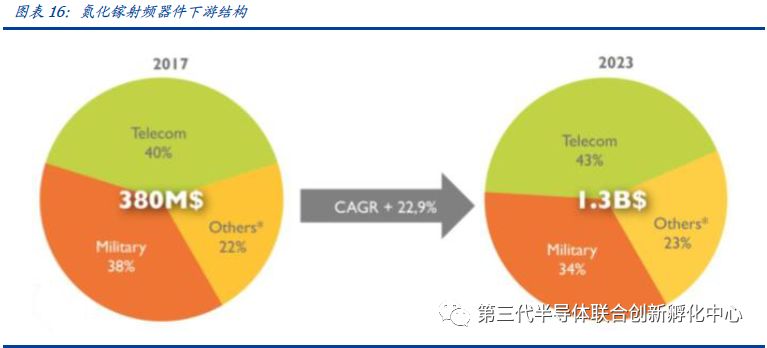
Gallium Nitride RF devices are growing rapidly, with a compound annual growth rate of 23%, and the overall downstream market structure remains stable. According to data from research firm Yole Development, the Gallium Nitride RF market size was $380 million in 2017 and is expected to grow to $1.3 billion by 2023, with a compound annual growth rate of 22.9%. The overall downstream application structure remains stable, mainly dominated by communications and military applications, which together account for about 80%.
▌Silicon Carbide: Core Material for Power Devices, Driving Growth in New Energy Vehicles
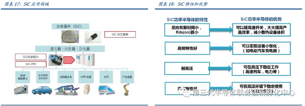
Silicon Carbide is mainly used in high-power high-frequency power devices. Devices such as diodes, MOSFETs, and IGBTs made from SiC are expected to replace Si in automotive electronics in the future. Currently, SiC semiconductors are still in the early stages of development, and dislocations in the substrate during wafer growth can lead to a decline in the reliability of SiC devices. On the other hand, the difficulty of wafer growth leads to high prices for SiC materials, and significant technical improvements will be needed before widespread application is achieved.
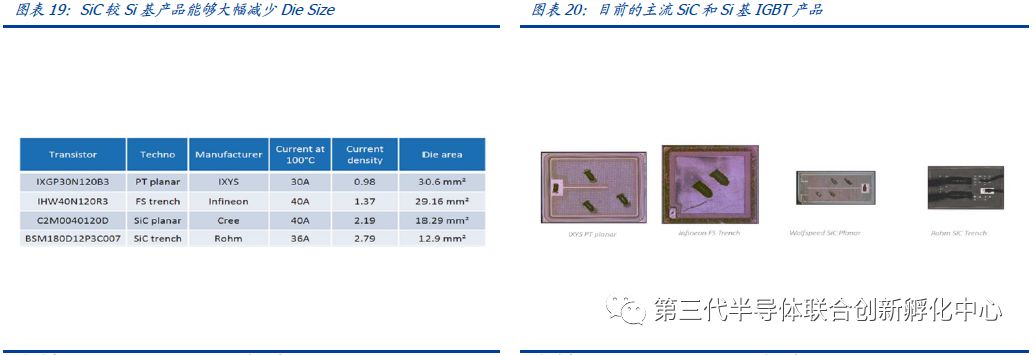
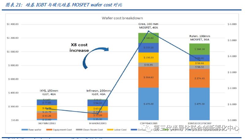
Die Size and cost are the core variables for the industrialization of Silicon Carbide technology. Comparing the current mainstream 1200V silicon-based IGBTs and silicon carbide-based MOSFETs, we find that SiC-based MOSFET products can significantly reduce die size while performing better than Si-based products. However, the biggest obstacle remains wafer cost; according to Yole Development estimates, the cost per wafer for SiC is 7-8 times higher than that of Si-based products.
Research firm IHS predicts that by 2025, the market size for SiC power semiconductors is expected to reach $3 billion. In the next decade, SiC devices will begin to be widely applied in industrial and electric vehicle fields. Looking at the global SiC market, power electronics accounted for the largest market share from 2016 to 2017. The main driver of growth in this market is the increasing use of SiC devices in power supplies and inverters.
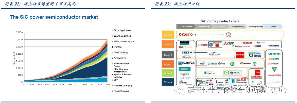
Recently, the industrialization progress of SiC has accelerated, with upstream supply chains beginning to expand and secure sources. Based on the announcements from CREE, we can find that the industrialization progress of Silicon Carbide has begun to accelerate, with midstream manufacturers like ST and Infineon starting to secure upstream wafer sources:
➢ January 2019 announcement: CREE signed a multi-year $250 million production supply agreement with ST, under which Wolfspeed will supply 150mm SiC wafers to ST.
➢ October 2018 announcement: CREE announced an $85 million long-term agreement to produce and supply SiC wafers for a leading power equipment company whose name has not been disclosed.
➢ February 2018 announcement: CREE signed a $100 million long-term supply agreement with Infineon to provide SiC wafers for products such as photovoltaic inverters, robotics, charging infrastructure, industrial power supplies, traction, and variable-speed drives.
Disclaimer: This article is compiled based on relevant reports from GuoshengSecurities, with copyright owned by the author. The views expressed in this article are for discussion purposes only and do not constitute any investment advice, nor do they represent the position of this public account. If there are any objections, please feel free to contact the International Third Generation Semiconductor Union Space.
5G CommunicationGaN RFIndustry Development Report
To purchase a printed version of the report
Please add the WeChat assistant
To get more information about the report