Welcome FPGA engineers to join the official WeChat technical group.
ClickBlue TextFollow us at FPGA Home – the largest FPGA engineer community in China
Generally, there are no issues with soldering I2C devices; following the device manual step by step usually leads to success. However, if such a simple thing fails to yield the desired results after repeated checks, troubleshooting, and verifying every command and data sent and received, what should be done?
This article focuses on I2C devices, explaining how to resolve issues with data communication between the I2C master and slave, particularly emphasizing problems caused by unreasonable hardware design or non-standard I2C device design leading to bus faults. It will analyze phenomena and propose solutions. Cases where data cannot be obtained due to uninitialized registers or commands during device initialization will not be detailed.
1 Basic Usage of I2C
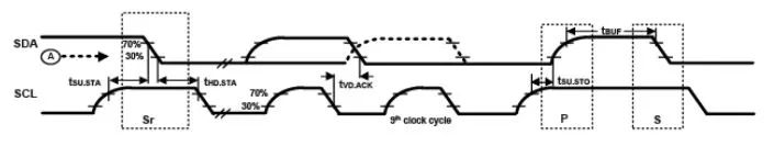
The I2C bus is a simple, bidirectional two-wire synchronous serial bus. All masters generate their own clock on the SCL line to transmit messages on the bus, while the SDA line transmits each byte, which must be 8 bits long. The number of bytes that can be sent in each transmission is unlimited, but each byte must be followed by an acknowledgment bit. In idle state, both SCL and SDA are high.
Typically, some low-power I2C devices can use pull-up outputs on chip pins for normal data communication. Other I2C devices may require an external pull-up resistor on the bus, in which case the corresponding I/O should be configured as open-drain output, and other configurations should follow the chip manual’s standard.
2 Summary of Hardware Issues
2.1 Unable to Pull Pins High or Low Normally
First, ensure that the SDA and SCL pins can be pulled high and low. The detection method is to directly control the I/O port output to low/high levels via software and measure the pin voltage to see if it can output the corresponding state according to the chip pin settings.
If the pins cannot be pulled low, check for cold solder joints, broken pull-up resistors, whether the I2C device is functioning normally, or if the chip pins are damaged, ensuring that they can be pulled high or low normally.
2.2 Electrical Characteristics Not Met
If the pins can be pulled high and low normally but data cannot be read, it is usually suggested to replace the resistor with a lower value based on the load current.
To understand the reasons in detail, refer to the electrical characteristics of the I2C device. Most I2C device electrical characteristics are roughly shown in the following figure.
This section primarily discusses the longest and shortest times for pulling levels high and low, as well as the threshold and duration for high and low levels.
In hardware design, to reduce microcontroller power consumption and protect chip pins, resistor values are usually set relatively high while meeting load current and capacitance requirements. If multiple I2C devices are connected to the same bus, even with correct I/O port configurations, it may lead to insufficient driving capability.
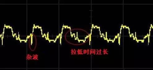
The symptoms include insufficient pull-up voltage, and excessive time consumption during the pull-up and pull-down processes. These two issues often result in the data line and clock line: short high voltage duration during pull-up; short low voltage duration during pull-down. Using an oscilloscope to capture the waveform shows spikes, sloped waves, and noise that do not conform to I2C device electrical characteristics; from the data perspective, the high level duration on the data line is too short, rise time is too long, fall time is too long, etc., exceeding the effective values of the device’s electrical characteristics. A typical noise graph is shown below.
If such abnormalities occur, it is recommended to replace with a smaller resistor to enhance bus driving capability and improve level transition speed. It should be noted that each MCU has a different current tolerance, and reducing the resistor should avoid exceeding the maximum current that the respective pin can handle.
3 SDA Deadlock
If the data from the I2C device can occasionally be correctly retrieved but still results in bus read/write errors when sending data or commands, it may encounter the deadlock issue described below. During a deadlock, the data line is pulled low, preventing the master from pulling it high. Deadlocks generally occur on the slave side and involve the data line. Since the I2C bus is shared, if it needs to be determined whether it is a slave deadlock, refer to the following two diagrams and test with series resistors.
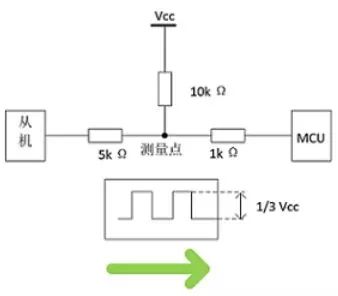
As shown in the figure above, if the slave is deadlocked, the voltage detected is 1/3 Vcc.
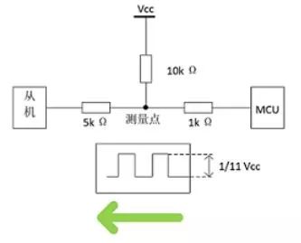
As shown in the figure above, if the master is deadlocked, the voltage detected is 1/11 Vcc. Based on this principle, the specific location of the deadlock can be accurately determined, with multiple sensors locating based on a similar method.
3.1 Repeated Restarts Leading to Deadlock
3.1.1 Phenomenon
If a device needs to restart repeatedly, it is likely that the SDA is locked when the slave device returns data. The specific reason is that the slave device has not finished sending data when the master clock disappears, and the slave waits for the clock signal. If the MCU restarts without resetting the slave device’s power, the slave continues to wait for the MCU’s clock signal, causing data to be held, and the bus cannot complete data communication.
3.1.2 Solution
To solve the deadlock caused by restarts, one method can be similar to the RT-Thread driver solution, providing 9 clock signals during system reset to release the bus deadlock; another method is to power off the slave device during initialization when the reset button is pressed, which requires pin control.
3.1.3 9 Clock Signals
During the read/write operations of I2C devices, if the slave holds the bus during the MCU’s abnormal reset, it leads to SDA deadlock, which occurs in two stages: slave response stage and slave data sending stage. The following will explain the clock signals for these two types of anomalies and summarize other reasons to draw conclusions.
(a) Slave Response Stage
After the MCU sends the address following the start signal and receives a response from the slave device, it prepares to return data. At this moment, the slave pulls the SDA signal low. If the MCU resets abnormally, the SCL stops sending clock signals, and the slave waits for the clock signal from the MCU, leading to the phenomenon of holding and pulling SDA low. To unlock SDA, the slave needs 9 clock signals to complete the response and release SDA.
(b) Slave Data Sending Stage
If the slave has completed the response and begins to return data to the MCU. This data consists of eight bits, each of which may be low. If the MCU resets abnormally during the low bits, it stops sending clock signals, and the slave waits for the clock signal from the MCU, leading to the phenomenon of holding and pulling SDA low. To unlock SDA, the slave needs 1-8 clock signals to complete the data response and release SDA.
(c) Other Situations
After a complete 8-bit data transmission by the slave, it waits for the MCU’s response. Even if it belongs to the MCU, the slave no longer holds SDA, and without a clock, data communication stops.
During the master sending data stage, the bus is owned by the master. If the master malfunctions, data communication stops, and the bus is released. Therefore, in these situations, there is no SDA deadlock.
(d) Conclusion
In summary, to unlock SDA, the slave needs at most 9 clock signals, meaning that after an abnormal reset, the MCU must send at least 9 clock signals to complete the unlocking of the I2C bus’s SDA. Therefore, RT-Thread avoids such issues by checking the bus during the I2C driver initialization to determine if unlocking is necessary; if so, it proceeds to unlock, ensuring that I2C devices do not fail in data communication due to this issue.
3.2 Multiple I2C Devices Leading to Deadlock
In addition to abnormal resets causing deadlocks, multiple I2C devices can also cause mutual interference. Generally, devices of the same slave address should not be connected to the same bus, but aside from that, some I2C devices are not designed according to standard I2C bus protocols. Under the premise of shared I2C bus, some devices will respond as long as there is a slave address on the bus. This erroneous response from the slave can cause various I2C bus anomalies and even hold the bus in a deadlock state.
The solution for such non-standard I2C devices is to use a separate bus to avoid interference or to control the power with a separate pin.
Source: RT-Thread

Welcome communication engineers and FPGA engineers to follow our public account.

The Largest FPGA WeChat Technical Group in the Country
Welcome everyone to join the national FPGA WeChat technical group, which has tens of thousands of engineers, a group of engineers passionate about technology. Here, FPGA engineers help each other and share knowledge, creating a strong technical atmosphere! Hurry up and invite your friends to join!!

Press and hold to join the national FPGA technical group!
FPGA Home Component City
Advantageous component services, please scan to contact the group owner: Jin Juan Email: [email protected] Welcome recommendations to purchasing
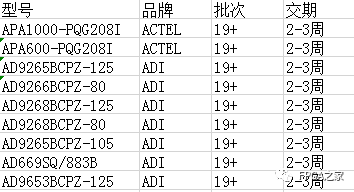
ACTEL, AD part advantageous ordering (operating full series):
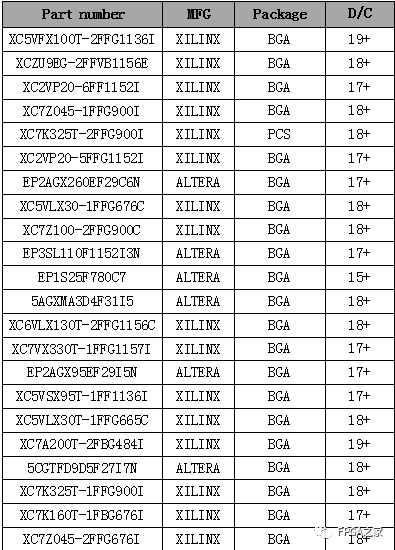
XILINX, ALTERA advantageous stock or ordering (operating full series):
(The above devices are part models, for more models please consult the group owner Jin Juan)
Service Philosophy: FPGA Home component self-operated city aims to facilitate engineers in quickly and conveniently purchasing components. After years of dedicated service, our customer service is spread across large domestic listed companies, military research units, and small to medium enterprises. Our biggest advantage is emphasizing service first, and achieving fast delivery and favorable prices!
Direct brands: Xilinx, ALTERA, ADI, TI, NXP, ST, E2V, Micron, and over a hundred component brands, especially skilled in handling embargoed components from the US to China. We welcome engineer friends to recommend us to purchasing or consult us directly! We will continue to provide the best service in the industry!

Official acknowledgments for FPGA technology group brands: Xilinx, Intel (Altera), Microsemi (Actel), Lattice, Vantis, Quicklogic, Lucent, etc.