)
Professor Wei Chen and others from the National University of Singapore published a paper titled “Doping-tunable charge ordering in semiconducting single-layer Cr2Se3” in the journal Science Advances.
This study achieved real-space observation of doping-tunable granular charge ordering in the semiconductor single-layer Cr₂Se₃ using scanning tunneling microscopy (STM). Cr₂Se₃ is a transition metal chalcogenide (TMC) of the hexagonal group, and the observed lattice distortion, modulation of the band gap at the Fermi level (E_F), and the STM contrast reversal at low temperatures indicate the origin of the charge order. The semiconductor properties of Cr₂Se₃ allow for the modulation of charge order through doping: hole doping suppresses charge order, while electron doping alters the charge order pattern, ultimately forming a periodic 3√3×3√3 charge density wave (CDW) phase. This finding not only provides a new perspective for understanding the interaction between doping and charge order in two-dimensional materials but also lays the foundation for the development of novel electronic devices based on Cr₂Se₃.
Background
Charge density waves (CDWs) are a type of charge ordered phase that provide an important framework for exploring electron-electron interactions, electron-phonon coupling, and quantum phase transitions. In CDW materials, the carrier density significantly affects the ground state, typically modulated by doping foreign ions on a macroscopic or mesoscopic scale. However, atomic-scale visualization in undoped CDW systems remains rare. This study focuses on Cr₂Se₃, a hexagonal transition metal chalcogenide, achieving direct observation of doping-tunable charge order using STM technology.
Main Content
The research team synthesized high-quality single-layer Cr₂Se₃ films on single-crystal graphene using molecular beam epitaxy (MBE) technology. Through STM and STS techniques, granular charge order was observed in Cr₂Se₃ at low temperatures, exhibiting contrast reversal under positive and negative bias, which is a typical feature of charge order. Additionally, non-contact atomic force microscopy (nc-AFM) verified the lattice distortion associated with the charge order. The study found that the semiconductor properties of Cr₂Se₃ allow for the modulation of charge order through doping: hole doping suppresses charge order through defect aggregation, while electron doping alters the charge order pattern by changing the position of the Fermi level, ultimately achieving a periodic 3√3×3√3 CDW phase on single-layer graphene.
Summary of Experimental Details
In the experiment, the research team first synthesized single-layer Cr₂Se₃ films in an ultra-high vacuum MBE chamber integrated with the AFM system. The substrates used included cleaved single-crystal graphite and epitaxial graphene on 4H-SiC(0001).
Innovations
-
Atomic-scale observation of charge order: Achieved the first atomic-scale direct observation of doping-tunable charge order in single-layer Cr₂Se₃.
-
Doping control of charge order: Achieved electron doping control of Cr₂Se₃ charge order by changing the substrate work function, observing the transition from non-periodic to periodic charge order.
-
Discovery of periodic CDW phase: Discovered a periodic 3√3×3√3 CDW phase in Cr₂Se₃ on single-layer graphene, providing a new perspective for understanding the formation mechanism of CDWs.
-
Application of STM contrast reversal: Utilized the STM contrast reversal phenomenon to further confirm the existence of CDWs and enhanced the visualization of CDW features through image processing techniques.
Conclusion
This study achieved direct observation of doping-tunable charge order in the semiconductor single-layer Cr₂Se₃ using STM technology, revealing the different effects of hole doping and electron doping on charge order. The results not only provide a new perspective for understanding the interaction between doping and charge order in two-dimensional materials but also lay the foundation for the development of novel electronic devices based on Cr₂Se₃.
Results and Discussion
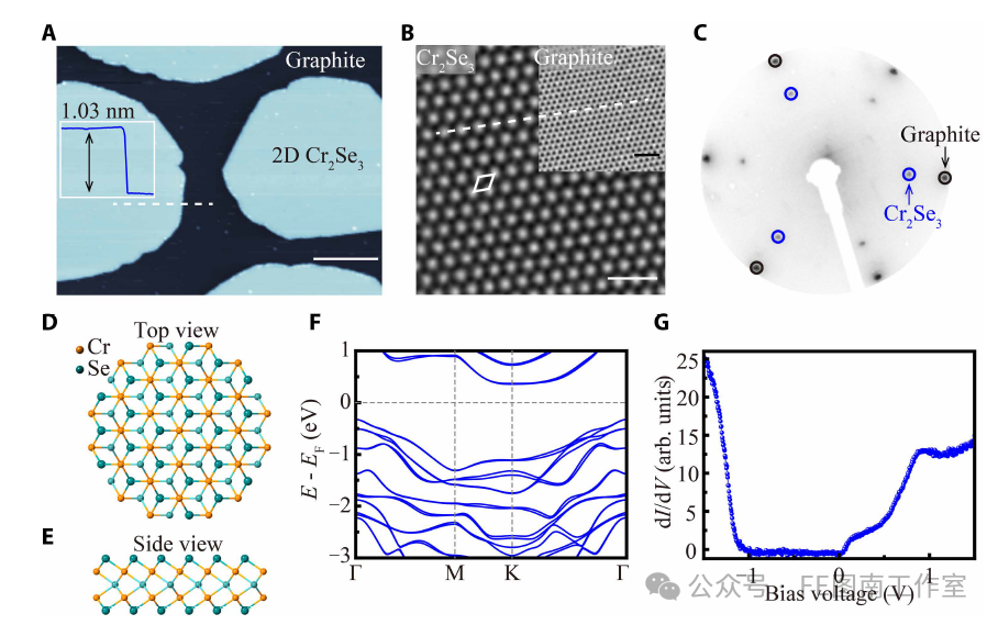 Figure 1. MBE growth and crystal structure of single-layer Cr2Se3 on a graphite substrate. (A) Large-scale STM morphology image of single-layer Cr2Se3, with the inset showing an STM line scan profile along the white dashed line, indicating a thickness of 1.03 nm (VS=2V, I=5pA, T=77K). Scale bar 36 nm. (B) nc-AFM image of Cr2Se3, with the tip height set relative to the set point height z=-170 pm (VS=0.2V, I=20pA), with the white rhombus outlining the Cr2Se3 unit cell. Scale bar 1 nm. The inset shows an atomic resolution STM image of the graphite substrate where Cr2Se3 was grown (VS=0.5V, I=50pA), scale bar 1 nm, with the white dashed line indicating the crystallographic alignment of Cr2Se3 with the graphite substrate. (C) LEED diffraction pattern of the Cr2Se3/graphite sample, with blue and black circles marking the Bragg peaks of Cr2Se3 and graphite, respectively. (D-E) Stick model of Cr2Se3: (D) top view and (E) side view. (F) DFT calculated band structure of isolated single-layer Cr2Se3, showing its semiconductor properties. (G) Wide bias dI/dV spectrum obtained on Cr2Se3/graphite, showing the band gap below the Fermi level (VS=1.5V, I=2nA, T=4.3K, lock-in oscillation amplitude Vmodu=10mV). arb. units are arbitrary units.
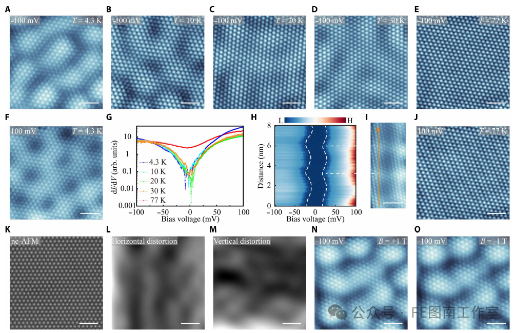 Figure 2. Charge ordering in single-layer Cr2Se3 on a graphite substrate. (A-E) STM images of single-layer Cr2Se3 obtained at different temperatures: (A) 4.3K, (B) 10K, (C) 20K, (D) 30K, and (E) 77K (VS=-100mV). Scale bars are all 1.6nm. (F) STM image of the same area as (A) but with opposite bias (VS=100mV, T=4.3K). (G) Temperature dependence of the low-bias dI/dV spectrum of Cr2Se3, showing a small band gap appearing at EF as the temperature decreases [VS=-100mV, I=500pA, T=4.3K (blue), 10K (cyan), 20K (green), and 30K (red); Vmodu=1mV]. (H) Spatially resolved dI/dV spectrum obtained along the orange arrow in (I), with the tip height set to z=0pm (relative to the set point height VS=-100mV, I=500pA, Vmodu=1mV). The white dashed line indicates the spatial modulation of the band gap edge caused by charge ordering. (I) STM image of the area where the spatially resolved dI/dV spectrum in (H) was collected (VS=100mV, I=100pA). Scale bar 2nm. (J) STM image of the same area as (E) but with opposite bias (VS=100mV, T=77K). (K) nc-AFM image of Cr2Se3 for lattice distortion measurement (z=-170pm relative to the set point height, VS=-100mV, I=10pA). Scale bar 1.6nm. (L-M) Lattice distortion maps calculated based on the local atomic positions in (K): (L) horizontal and (M) vertical directions. Scale bars are all 1.6nm. (N-O) STM images of Cr2Se3 obtained under different magnetic fields: (N) B=1T and (O) B=-1T. Scale bars are all 1.6nm.
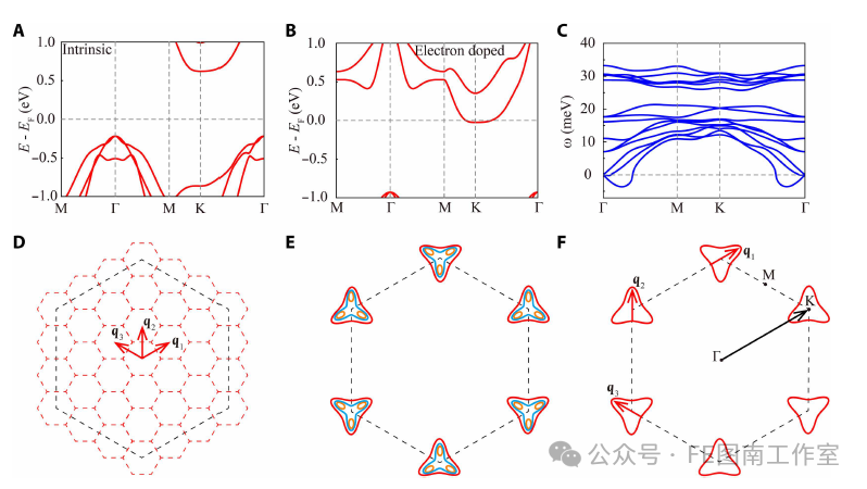 Figure 3. Doping tunability of charge ordering in single-layer Cr2Se3. (A) STM image of single-layer Cr2Se3/graphene (VS = -100 mV, I = 10 pA), showing suppressed charge order at the island edge (upper right area of the white dashed line). Scale bar 1.6 nm. (B) nc-AFM image of the same area as (A), with the white dashed line marking the same region. (C) Magnified view of the area framed by the white dashed line in (A), showing the II region 2×2 supercell (red rhombus) and suppressed charge order. Scale bar 0.52 nm. (D) LC PD curve and (E) spatially resolved dI/dV spectrum obtained along the red arrow in (A) (Vmodu = 10 meV), both showing upward band bending at the island edge. Tip heights: (D) z=100 pm and (E) z=150 pm (relative to the set point VS=-100 mV, I=10 pA). (F-I) Occupied state STM images of Cr2Se3 on 4H-SiC(0001) with (F) four layers, (G) three layers, (H) two layers, and (I) single-layer graphene (VS=-200 mV). Scale bars are all 1.6 nm. (J) STM image of Cr2Se3/MLG in the same area as (I) (VS=100 mV), showing contrast reversal. (K) Relationship between grain density (blue) and substrate work function (red) as a function of the number of graphene layers. (L) Fourier transform of (I), with red and blue circles marking the CDW peak and Bragg peak, respectively. (M) Relationship of the intensity ratio of the 3√3×3√3 peak (I3√3×3√3) to the Bragg peak (IBragg) as a function of bias in different conductivity mapping Fourier transforms. (N) STM image processed for contrast reversal of only the CDW component in (L).
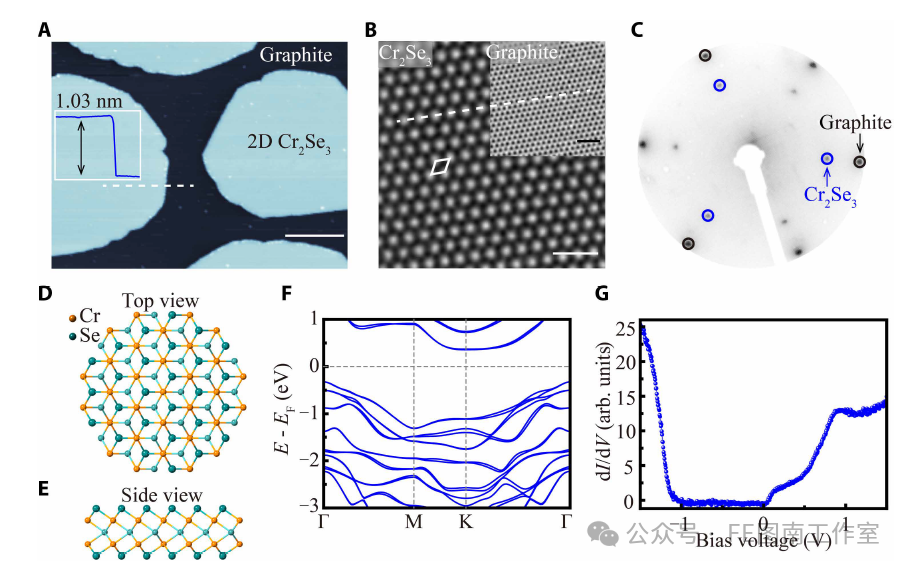 Figure 4. Mechanism of charge ordering formation in Cr2Se3. (A and B) DFT calculated band structures of (A) intrinsic and (B) electron-doped Cr2Se3. (C) DFT calculated phonon dispersion relation of electron-doped Cr2Se3 in the normal phase, observing imaginary frequency modes near the Γ point. (D) Brillouin zones of the normal phase (black) and 3√3×3√3 CDW phase (red), with the CDW wave vector indicated by red arrows. (E) Simulated constant energy surface at the Fermi level for electron-doped Cr2Se3 in the normal phase, estimating electron doping levels of 0.002 e−/unit cell (orange), 0.029 e−/unit cell (blue), and 0.058 e−/unit cell (red). (F) Simulated constant energy surface at the Fermi level, with the magnitude of the nested vector (red arrow) being |qi| = 1/3 |Γ-K|.References:
Sisheng Duan et al., Doping-tunable charge ordering in semiconducting single-layer Cr2Se3. Sci. Adv. 11, eadx8310 (2025).
10.1126/sciadv.adx8310
FE图南工作室