13.2.2.2
PLL2 Phase-Locked Loop
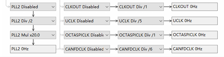
The PLL output is mainly used for system clock (ICLK) and others, while PLL2 is primarily used for some important peripherals, providing them with a stable clock separately. Here, we do not use PLL2.
PLL2 section in the FSP clock configuration diagram:
13.2.3
System Clock Area
See the marked area ③ in the diagram.
The system clock refers to ICLK. The system clock (#ICLK) is the operating clock for the CPU, DMAC, DTC, Flash, and SRAM. The clock source for ICLK can be selected from MOSC, SOSC, HOCO, MOCO, LOCO, XTAL, PLL (excluding PLL2). We only need to configure the “ClockSrc” in the clock configuration diagram to make a selection.
For different Enlightenment development boards, we generally refer to the main frequency of the main chip to set the system clock:
-
The RA6M5 has a main frequency of 200MHz, so its ICLK is generally set to 200MHz.
-
The RA4M2 has a main frequency of 100MHz, so its ICLK is generally set to 100MHz.
-
The RA2L1 has a main frequency of 48MHz, so its ICLK is generally set to 48MHz.
Note that when setting the system clock, we must not exceed the frequency range specified in the chip manual; exceeding it may cause the chip to operate unstably, leading to overheating, program runaway, etc.
Of course, this area does not only include the system clock (ICLK) but also includes other internal bus clocks:
-
Peripheral module clocks: PCLKA, PCLKB, PCLKC, PCLKD
-
FlashIF clock: FCLK
-
External bus clock: BCLK
This needs to be analyzed based on specific chips; for example, RA4M2 and RA2L1 do not have BCLK.
13.2.4
Dedicated Peripheral Independent Clock Area
See the marked area ④ in the diagram.
This area mainly contains dedicated clocks for some important peripherals, such as USB peripheral clock (#UCLK), OSPI peripheral clock (OCTASPICLK), and CANFD peripheral clock (CANFDCLK). Some RA chips do not support these peripherals, and generally, there will not be corresponding dedicated clocks for those peripherals.
In addition to dedicated peripheral clocks, there is also a #CLKOUT, which is generally available in all MCUs. CLKOUT is a clock signal output that can output internal clock signals to corresponding external pins, thus providing clock drive signals for other external circuit modules. Sometimes we can also use this CLKOUT to measure its clock frequency with an oscilloscope, and based on some clock division configurations, we can calculate the current operating main frequency of the chip.
13.3
Setting System Clock Library Function
The clock tree described above corresponds to the configuration function as follows. This function is excerpted from the FSP library file ./ra/fsp/src/bsp/mcu/all/bsp_clocks.c. For ease of reading, this chapter has removed some temporarily unused, compiled code and translated the English comments into Chinese. This function directly operates the registers; for the register part, please refer to the “8. Clock Generation Circuit” section of the data manual for the register description.
List 1:
Code Listing 14-1 bsp_clock_init Clock Configuration Library Function
Swipe left and right to view the full content
/*******************************************************************************************************************/ /** * Initializes system clocks. Makes no assumptions about current register settings. **********************************************************************************************************************/ void bsp_clock_init(void) { /* Unlock CGC and LPM protection registers. */ R_SYSTEM->PRCR = (uint16_t) BSP_PRV_PRCR_UNLOCK; /* Enable flash cache; do not disable it when running from flash. On these MCUs, it is not necessary to disable the flash cache when adjusting the operating power mode. */ R_BSP_FlashCacheEnable(); /* Initialize variables to store system clock frequency. */// Store, for example: g_clock_freq[BSP_CLOCKS_SOURCE_CLOCK_MAIN_OSC] = BSP_CFG_XTAL_HZ; bsp_clock_freq_var_init(); // Main macros come from bsp_clock_cfg.h /* Configure main oscillator driver. */ R_SYSTEM->MOMCR = BSP_PRV_MOMCR; /* Set main oscillator wait time. */ R_SYSTEM->MOSCWTCR = (uint8_t) BSP_CLOCK_CFG_MAIN_OSC_WAIT; /* If the sub-clock oscillator starts on reset, stop before configuring the sub-clock driver. */ if (0U == R_SYSTEM->SOSCCR) { /* Stop the sub-clock oscillator to update SOMCR register. */ R_SYSTEM->SOSCCR = 1U; /* Allow at least 5 SOSC clock cycles of stop interval before configuring drive capacity and restarting the sub-clock oscillator. */ R_BSP_SoftwareDelay(BSP_PRV_SUBCLOCK_STOP_INTERVAL_US, BSP_DELAY_UNITS_MICROSECONDS); } /* Configure sub-clock driver when the sub-clock is not running. */ R_SYSTEM->SOMCR = ((BSP_CLOCK_CFG_SUBCLOCK_DRIVE << BSP_FEATURE_CGC_SODRV_SHIFT) & BSP_FEATURE_CGC_SODRV_MASK); /* Restart the sub-clock oscillator. */ R_SYSTEM->SOSCCR = 0U; /* First start all clocks used by other clocks. */ R_SYSTEM->HOCOCR = 0U; R_SYSTEM->MOSCCR = 0U; /* Wait for the main oscillator to stabilize. */ FSP_HARDWARE_REGISTER_WAIT(R_SYSTEM->OSCSF_b.MOSCSF, 1U); /* Start clocks that require other clocks. At this point, if needed, all relevant clocks are running and stable. */ /* Configure PLL registers. */ R_SYSTEM->PLLCCR = (uint16_t) BSP_PRV_PLLCCR; // PLL's division factor and multiplication factor R_SYSTEM->PLLCR = 0U; /* Wait for PLL to stabilize. */ FSP_HARDWARE_REGISTER_WAIT(R_SYSTEM->OSCSF_b.PLLSF, 1U); /* Set source clock and divider. */ bsp_prv_clock_set_hard_reset(); // System clock source selection, other clock division factor selection /* Configure BCLK (if it exists on the MCU). */ R_SYSTEM->BCKCR = BSP_CFG_BCLK_OUTPUT - 1U; R_SYSTEM->EBCKOCR = 1U; /* Configure CLKOUT. */ uint8_t ckocr = BSP_CFG_CLKOUT_SOURCE | (BSP_CFG_CLKOUT_DIV << BSP_PRV_CKOCR_CKODIV_BIT); R_SYSTEM->CKOCR = ckocr; ckocr |= (1U << BSP_PRV_CKOCR_CKOEN_BIT); R_SYSTEM->CKOCR = ckocr; /* Lock CGC and LPM protection registers. */ R_SYSTEM->PRCR = (uint16_t) BSP_PRV_PRCR_LOCK; }

Need Technical Support?
If you have any questions regarding the use of Renesas MCU/MPU products, you can identify the QR code below or copy the URL into your browser to enter the Renesas Technical Forum to find answers or obtain online technical support.

https://community-ja.renesas.com/zh/forums-groups/mcu-mpu/
To be continued
Recommended Reading
CGC Clock Control – Practical Guide to Renesas RA Series FSP Library Development (29)
CGC Clock Configuration Block Diagram Analysis – Practical Guide to Renesas RA Series FSP Library Development (30)

Clock Sources – Practical Guide to Renesas RA Series FSP Library Development (31)