EMMC (Embedded Multi Media Card) is a standard specification for embedded storage primarily aimed at products like mobile phones or tablets, established by the MMC Association. EMMC integrates a controller within the package, providing a standard interface and managing flash memory.The schematic for the 8-bit data signal is shown in Figure 8-38, while the address and control signals are shown in Figure 8-39, and the power signals are shown in Figure 8-40. The RK3588 EMMC controller has the following features:
1. Compatible with specifications 5.1, 5.0, 4.51, 4.41;
2. Supports three data bus widths: 1bit, 4bit, and 8bit;
3. Supports HS400 mode, backward compatible with HS200, DDR50, and other modes;
4. Supports CMD Queue.
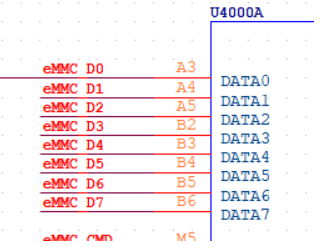
Figure 8-38 EMMC Partial Data Signal Pins
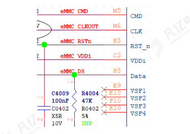
Figure 8-39 EMMC Partial Clock and Control Signals
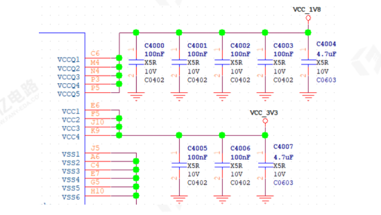
Figure 8-40 EMMC Partial Power Pins
The RK3588 eMMC interface is multiplexed with the FSPI Flash interface (a multiplexed port FSPI_M0). When designing the eMMC interface, please follow the circuit diagram in reference Figure 8-41, which includes various power decoupling capacitors. When using eMMC, the boot code should be placed in the eMMC.
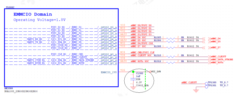
Figure 8-41 Recommended EMMC Circuit Connection Diagram
Recommendations for pull-up and pull-down design of the EMMC interface are shown in Table 8-4.
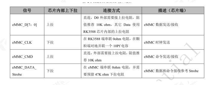
Table 8-4 EMMC Circuit Pull-Up and Pull-Down Design
1. When placing the EMMC controller’s pull-down resistors for the clock signal, they should be placed close to the pins; the clock signal needs to be ground processed, with a ground via every 200 mil, as shown in Figure 8-42.
2. The data signals, clock signals, and control signals of the EMMC need to maintain a 50-ohm impedance.
3. The filtering capacitors for each power pin of the EMMC should be placed close to the corresponding pins, ideally one capacitor per pin, as shown in Figure 8-43.
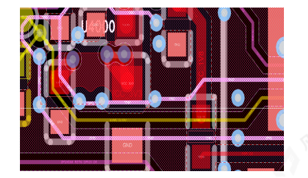
Figure 8-42 CLK Circuit Grounding Diagram
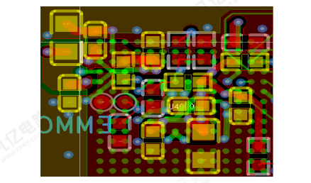
Figure 8-43 Power Filtering Capacitor Placement Diagram
5. The clock, data, and CMD signals need to be routed in a serpentine manner with a length error of less than 120 mil. The total length of the traces should not exceed 3500 mil.
6. The EMMC chip is packaged in a 0.5 pitch BGA package, which has many unused pins, allowing traces to be routed using the unused EMMC pins, reducing the spacing requirements for PCB manufacturing.
7. Minimize layer changes and vias for all EMMC signals, ideally not exceeding two vias. Before and after changing layers for EMMC signals, it is recommended that the reference planes be ground planes. Within a 30 mil range of signal vias (the center-to-center distance between vias), it is recommended to add ground return vias to improve the signal return path. Ground vias should connect the ground reference planes before and after the signal layer change.