
Abstract
Printed Circuit Boards (PCBs) are essential components in electronic devices, and their quality directly affects the performance and reliability of electronic products. During the PCB manufacturing process, defects such as open circuits, short circuits, and missing pads may occur due to process issues. To improve detection accuracy and efficiency, this paper utilizes Matlab image processing techniques, employing methods such as template matching, edge detection, and morphological processing to achieve automatic detection of PCB defects. Experimental results indicate that this method can effectively identify various defects in PCBs and achieve good results in binarization, image matching, and annotation.
Theory
PCB defect detection is primarily based on image processing technology, involving the following key steps:
1. Image Preprocessing
- Read the PCB image and convert it to grayscale.
- Use Gaussian filtering or median filtering to remove noise.
- Perform histogram equalization to enhance contrast.
2. Edge Detection
- Use operators such as Sobel and Canny to extract edge features of the PCB.
- Optimize edge detection results through morphological operations (dilation, erosion).
3. Template Matching
- Use a standard PCB image as a reference to match with the detected image.
- Calculate the structural similarity between the two (e.g., cross-correlation, mean squared error) to identify abnormal areas.
4. Defect Identification and Annotation
- Determine defect locations through connected component analysis.
- Use color to annotate defects, enhancing visualization.
Experimental Results
In the experiments, we used a set of standard PCB images and defective PCB images, applying the aforementioned methods for detection and comparing the detection effects of different algorithms. The experiments showed:
- Edge detection methods can effectively extract the wire contours of the PCB, but may produce false positives in noisy conditions.
- Template matching methods can accurately locate defects but require high computational resources.
- Morphological processing performs well in noise removal and enhancing target features.
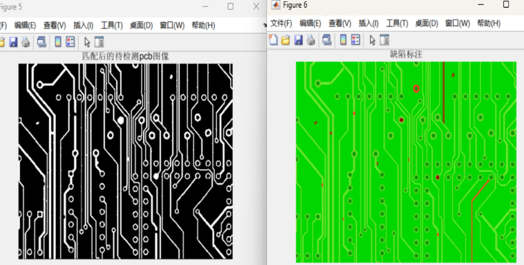
- The final detection results can clearly annotate defect areas, such as missing pads, fractures, and short circuits.
The table below shows a comparison of detection effects of different methods:
From the experimental results, it can be seen that the method combining template matching and morphological processing achieves better detection results.
Sample Code
clc; clear; close all;

% Read PCB image
pcb_img = imread('pcb_test.jpg');
gray_img = rgb2gray(pcb_img);

% Perform edge detection
edge_img = edge(gray_img, 'Canny');

% Morphological processing
se = strel('disk', 2);
morph_img = imdilate(edge_img, se);

% Read standard PCB image
template_img = imread('pcb_template.jpg');
template_gray = rgb2gray(template_img);
template_edge = edge(template_gray, 'Canny');

% Calculate difference
diff_img = abs(double(morph_img) - double(template_edge));

% Binarize defect area
threshold = 0.2;
defect_mask = diff_img > threshold;

% Annotate defects
defect_marked = pcb_img;
defect_marked(repmat(defect_mask, [113])) = 255; % Mark defects in red

% Display results
figure;
subplot(1,2,1); imshow(morph_img); title('Matched PCB Image for Detection');
subplot(1,2,2); imshow(defect_marked); title('Defect Annotation');
Related Technologies
❝
- Gonzalez, R. C., & Woods, R. E. (2018). Digital Image Processing (4th Edition). Pearson.
- Jain, A. K. (1989). Fundamentals of Digital Image Processing. Prentice-Hall.
- Davies, E. R. (2012). Computer and Machine Vision: Theory, Algorithms, Practicalities. Academic Press.
(The content of this article is for reference only; specific effects are subject to the images.)