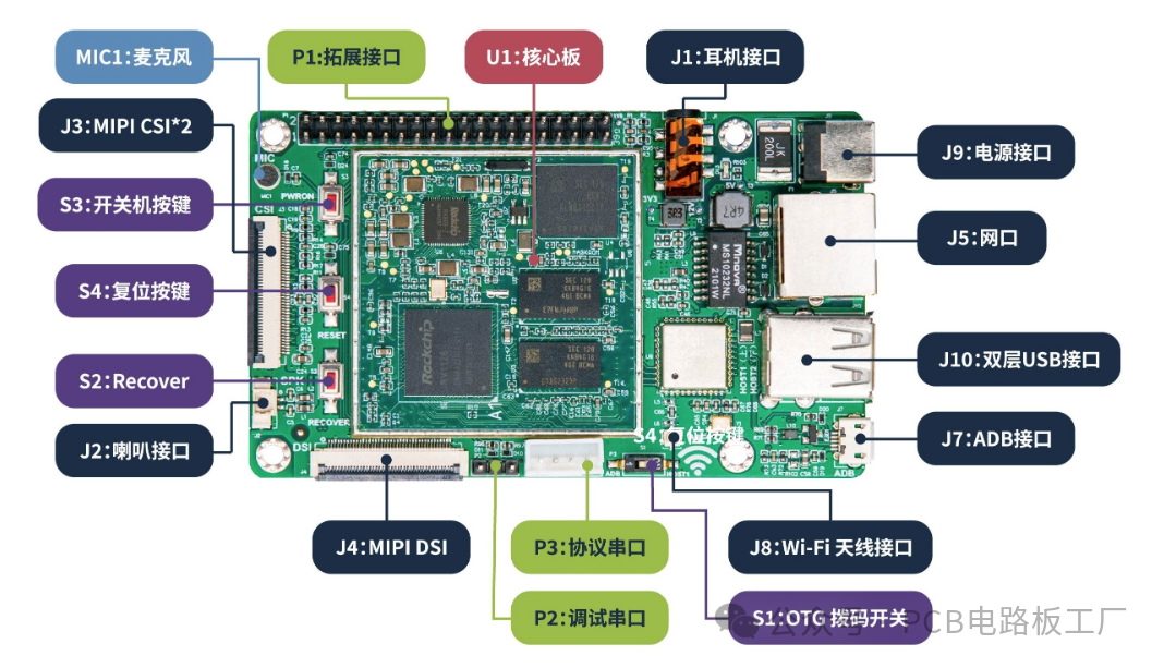
When designing PCBs, the design requirements for common hardware interfaces are crucial for ensuring circuit performance and stability. Below are some common hardware interface PCB design requirements:

1. USB Interface Design Requirements
① Total length control: Keep it within 1800 mils as much as possible.
② Differential pair characteristic impedance: 90Ω.
③ Power pin trace width: ≥30 mils.

2. VGA Interface Design Requirements
① Layout: Typically in a straight line or L-shape.
② Signal line thickening: R, G, B, HSync, and VSync signal lines should be thickened to 15 mils and grounded.
③ Analog signal processing: It is necessary to separate the analog signal ground (VGAGND) on the ground layer.
3. SATA Interface Design Requirements
① Via control: Avoid vias as much as possible, with a maximum of 2 vias.
② Differential pair control: Characteristic impedance is 90Ω.
③ Coupling capacitor placement: It is recommended to place them close to the connector and symmetrically.
4. Ethernet Interface (RJ45) Design Requirements
① Distance between transformer and RJ45: Keep it as short as possible, typically placed according to the signal flow direction.
② Reset circuit and Ethernet conversion chip: The reset circuit signal should be close to the Ethernet conversion chip, away from TX, RX, and clock signals.
5. PCIe Interface Design Requirements
① Differential pair layout: Arrange as closely as possible, keeping distance from other unrelated signals.
② Differential pair trace width and spacing: The two wires in each pair should have consistent width (e.g., 7 mils) and maintain a constant center-to-center distance (also 7 mils).
③ Length matching: The maximum allowable length difference between two differential lines should not exceed 5 mils.
6. Other Interface Design Requirements
LVDS and RGB interfaces: In LVDS PCB design, impedance requirements and length differences are proposed; in RGB PCB design, attention is emphasized on the placement of filter capacitors, series resistors for signal lines, and power routing for LCDs.
Interfaces such as SPI, UART, ULPI Interface (60 MHz), and USB 3.0: The PCB and packaging timing requirements for these interfaces must also be considered, for example, the PCB and packaging timing deviation for SPI should be within ±100 ps; the MIO tracking delay for UART should be less than 1.30 ns; the PCB and packaging delay for USB 2.0 should be maintained at 1.30 ns or less, ensuring that the delay deviation for data lines and clock lines is within ±100 ps.
Different types of hardware interfaces have specific requirements in PCB design, including but not limited to differential signal matching, impedance control, trace length deviation, via and GND via handling, AC coupling capacitor addition, and layer design.


Screenshots of Some Electronic Books

【Complete Set of Hardware Learning Materials Collection】
