1 Development and Classification of Data Acquisition Instruments
As shown in Figure 1, in vibration noise testing, we focus on the final test analysis results, such as the time-domain and frequency-domain characteristics of the signals. To analyze the data, we need to acquire it. Directly obtaining physical quantities is quite challenging, especially for high-frequency physical quantities like vibration noise. At this point, we need to use sensors to convert these physical quantities into easily measurable electrical signals.Typically, the electrical signals output by sensors are mainly voltage, current, and resistance signals, but these signals are still analog signals that can only be measured and analyzed using circuits, and cannot be analyzed using digital signal processing methods.At this time, a data acquisition instrument is required to convert the analog signals into digital signals, which can then be analyzed using digital signal processing methods in analysis software to obtain the results we need.

Figure 1 Composition of the Testing System
As shown in Figure 2, data acquisition instruments, or dynamic signal analyzers, have basically evolved from analog to digital. Early instruments not only had lower accuracy but also relied heavily on circuits for analysis functions, making them relatively simple. Different analyses sometimes required different instruments.With the advancement of digital signal processing and electronic circuit technology, dynamic signal analyzers have developed towards digitization, focusing more on converting sensor signals into digital signals, which are then analyzed and processed using software.At this time, the instruments often have higher integration, incorporating conditioning circuits into one unit, reducing connection links and improving testing reliability, and of course, accuracy is also increasing.Many modern instruments are no longer designed solely for high-precision and high-speed data acquisition; they gradually possess more powerful data analysis capabilities, ranging from simple index measurements or frequency spectrum feature analysis to complex fault identification and diagnosis functions that combine pattern recognition and artificial intelligence methods. There are increasingly more data acquisition and analysis systems targeting specific equipment, such as condition monitoring and fault diagnosis instruments for motor failures.

Figure 2 Development of Data Acquisition Instruments
The most common classification of data acquisition instruments is based on the number of channels of a single device, and many manufacturers design their product lines based on this classification. As shown in Figure 3, centralized systems are mainly used for laboratory or field measurements where measurement points are concentrated, such as fatigue strength tests. These types of acquisition instruments can have dozens to hundreds of channels, mostly in a plug-in card format, some with built-in CPUs and storage media, while others do not. Those without built-in capabilities often require faster data transmission capabilities.For field testing, especially for large engineering projects like bridges or railway engineering, each measurement section often has only a few or a dozen measurement points, and the distances between testing sections are often quite far.In such cases, low-channel distributed devices are typically used. These devices have fewer channels, and the types of sensors that can be connected to each channel are more flexible. Since these devices often operate in field environments, to reduce the workload of testing personnel, they often come with rechargeable batteries and can independently complete data acquisition and recording tasks based on preset tasks and logic.Many manufacturers also choose to use portable chassis-type acquisition devices to cover these two application scenarios. Portable chassis-type acquisition devices usually also use plug-in cards, with the number of channels and size falling between centralized and distributed systems.For situations like production lines where multiple devices need to perform vibration noise level inspections, handheld devices are typically used. These devices not only have fewer channels but also feature interactive screens and embedded data analysis software.The most common handheld devices are handheld vibration analyzers and sound level meters.
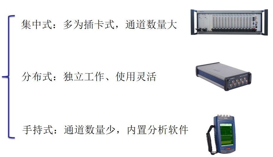
Figure 3 Classification of Data Acquisition Instruments
2 Common ADC Working Principles
No matter the stage or type of data acquisition instrument, a necessary function is to convert the sensor’s analog signal into a digital signal, which requires the use of an Analog-to-Digital Converter (ADC).Analog signals are continuous in both amplitude and time, while digital signals are discrete and have a limited number of bits. In simple terms, an ADC typically needs to perform two steps to achieve this conversion: sampling and quantization.Through sampling, the continuous analog signal is truncated into discrete signals, but at this point, it is still an electrical signal, representing a point on a continuous amplitude scale. It needs to be quantized to convert the electrical signal into a digital signal.Quantization can round the sampled values to the nearest integer multiple of the smallest unit, which is referred to as the quantization unit, as shown in Figure 4.
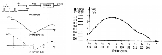
Figure 4 Sampling and Quantization
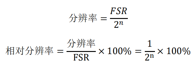
One of the most important parameters of an ADC is its resolution. The absolute resolution is related to the number of bits of the digital signal output by the ADC and the full-scale amplitude. It is equal to the full-scale range divided by 2 raised to the power of n, where n is the number of bits of the ADC. The higher the number of bits, the smaller the range and the better the resolution.Relative resolution can also be used to describe the accuracy of an ADC; it is the ratio of absolute resolution to the full-scale value, ignoring the effect of range on the size of the resolution.
A diagram intuitively illustrating the impact of the number of bits of an ADC is shown in Figure 5. This is a grayscale image, where the leftmost image is quantized from black to gray to white into 256 levels of gray values from 0 to 255. As we move to the right, the quantization levels gradually decrease. We can see that when it decreases to 128, the image quality is still acceptable, but when it decreases to 8, the color boundaries become obvious, and at 2, only a rough image can be seen, with details completely lost.
 Figure 5 Image Quantization
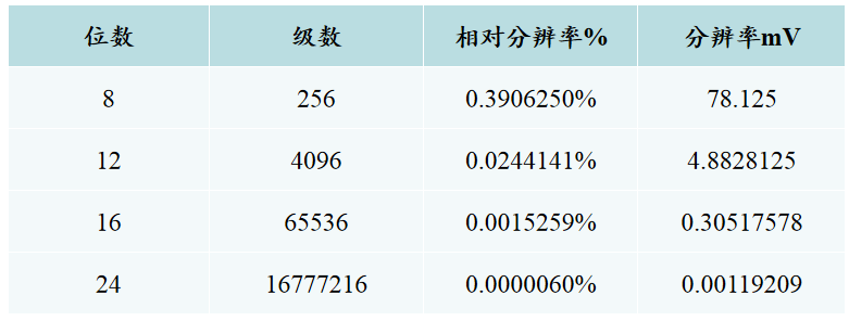
Taking the most commonly used ±10V range of data acquisition instruments as an example, comparing the resolution of different ADC bit depths, the signals output by testing sensors are generally in the mV range. Using 8-bit or 12-bit ADCs often results in the loss of signal detail features, while a 16-bit resolution is 0.3mV, which often does not meet the requirements in micro-vibration testing, as shown in Table 1.
Table 1 Resolution of ADC with Full Scale of ±10V
Analog-to-Digital Converters are used in many applications such as imaging and recording. The main types of ADCs include:
1) High-speed parallel comparator (Flash) ADC
2) Dual slope integrator ADC
3) Counter (ramp tracking) ADC
4) Successive approximation ADC
5) Σ-Δ modulator ADC
6) Pipelined ADC
7) Interpolating and folding interpolating ADC
In vibration noise testing equipment, the most commonly used are successive approximation and Σ-Δ types. The following sections mainly introduce the principles of these two types of ADCs.
2.1 Successive Approximation
The principle of successive approximation is relatively easy to understand. It can be equated to the following problem: suppose the mass of an object is between 0-255g, and we have a balance and 8 weights of 1g, 2g, 4g, 8g, 16g, 32g, 64g, and 128g. How can we quickly determine the mass of the object?We can easily think of placing the 128g weight first.If the balance indicates that the object is heavier, we keep the 128g weight; if not, we remove the 128g weight and place the 64g weight, using the same method to determine whether to keep or remove it, continuing until we determine the 1g weight, ultimately deducing the mass of the object based on the remaining weights on the tray.The mass of the object can be expressed in the following formula, where d is 0 or 1, with 1 indicating the weight is kept and 0 indicating it is not.

The working principle of a successive approximation ADC is similar to this problem. Figure 6(a) shows the structural diagram of a successive approximation ADC. The register output is compared with the input value Vin after being converted by a DAC. If the DAC output is greater than the input voltage, then di is 0; otherwise, it is 1. The number of comparisons made corresponds to the number of bits in the ADC, and the final comparison results are output. Figure 6(b) shows the conversion process of a 4-bit ADC.Of course, to improve conversion speed, the actual circuit diagram is more complex than this.
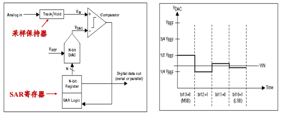
(a) (b)
Figure 6 Principle of Successive Approximation ADC
2.2 Σ-Δ Modulation
Before introducing the Σ-Δ ADC, we first need to discuss the concept of quantization error, which helps in better understanding the principle of Σ-Δ ADC.For an ideal N-bit ADC, its quantization process will produce quantization errors for DC input signals and quantization noise for AC input signals, as shown in Figure 7.To facilitate understanding, let’s first consider a simpler case: the maximum quantization error of an ideal N-bit ADC is equal to 1/2 of the smallest quantization unit. When the input signal linearly increases from zero to full scale, the quantization error appears as a peak-to-peak value equal to q, which is the voltage value corresponding to the smallest quantization unit. The quantization noise is equal to the effective value of this sawtooth wave. Through definite integration, we can obtain its effective value, as shown in equation (1-1). The quantization noise is only related to the ADC resolution and is independent of the signal amplitude and sampling rate. This means that regardless of how large the amplitude or how high the frequency of sampling, the quantization noise remains constant; it is a fundamental error that can only be reduced but not completely eliminated.
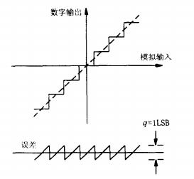
Figure 7 Quantization Noise

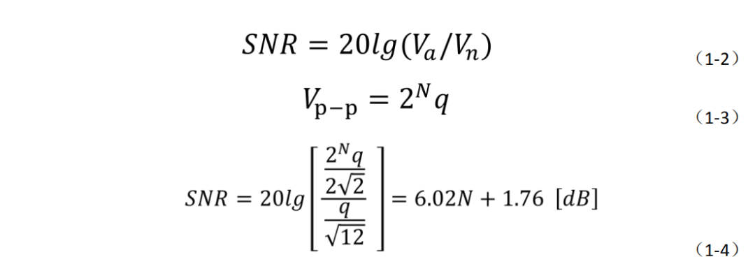
For an N-bit ADC, its theoretical signal-to-noise ratio (SNR) can be calculated as follows: assuming the ADC input is a full-scale sine wave signal, the SNR can be expressed as equation (1-2), where Va and Vn are the effective voltage values of the signal and quantization noise, respectively, and Vpp is the peak-to-peak value of the signal.Based on the previously introduced knowledge, we can derive equation (1-3), where all signal effective values are as shown in equation (1-1). Therefore, we can obtain the relationship between the ideal ADC SNR and the number of bits as shown in equation (1-4). This formula indicates that for each additional bit of ADC resolution, the SNR increases by 6dB.Conversely, an increase of 6dB in SNR is equivalent to an increase of one bit in ADC resolution. In the SNR formula, for a fixed input signal, the way to improve SNR is to reduce quantization noise.
As mentioned earlier, quantization noise is white noise, and its total effective value is independent of the sampling frequency.So, if we increase the sampling frequency, the quantization noise will be distributed over a wider frequency band, and the amplitude of the noise spectrum will decrease. Then, by using a low-pass filter to remove the unwanted parts, the effective value of the quantization noise will decrease, thus improving the SNR. This is the principle of oversampling to reduce noise power, as shown in Figure 8.Calculations show that for every fourfold increase in sampling rate, the SNR improves by 6dB, which is equivalent to increasing the ADC resolution by one bit.
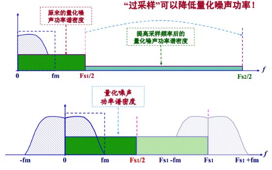
Figure 8 The Principle of Oversampling to Reduce Quantization Noise
Although analog signals are continuous signals, the sampled values of the signals are correlated.If the sampling rate is very high, the sampling intervals will be smaller, and the amplitude changes between adjacent sampling points will not be significant.If we quantize the difference between two adjacent points, it can also represent the information contained in the continuous signal. The essence of an ADC based on this idea is an incremental modulator, as shown in Figure 9.
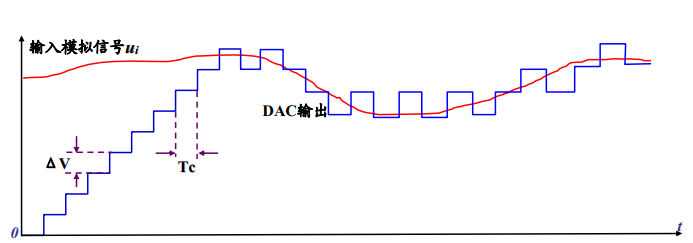
Figure 9 Principle of Incremental Modulator
If we only use an incremental modulator, large signal changes can exceed the quantization step δ, leading to slope overload where the signal changes cannot be tracked.To overcome this drawback, we can first integrate the signal and then perform incremental modulation, followed by a differentiation step before the final output to compensate for the signal changes caused by integration.Incremental is represented by δ, and integration or summation is represented by Σ, which is the origin of the name Σ-Δ ADC. Figure 10 shows the structure of a Σ-Δ ADC, where the differentiator and integrator used for incremental summation cancel each other out, leaving only the integrator to solve the slope overload problem.
Figure 10 Structure of Σ-Δ ADC
The working principle of the Σ-Δ modulator can also be described using the waveforms at points A, B, C, and D in its structure, as shown in Figure 11. When the input voltage VIN = 0, the voltage at point A is either +VREF or -VREF, and point B is the output of the integrator.Assuming the integrator input is +VREF, the integrator output will increase linearly. When the voltage at point B reaches the threshold for the latch comparator to flip, the latch comparator flips, and the output at point C becomes 1. The output D of a 1-bit DAC is +VREF, at which point the voltage at point A changes to VIN – (+VREF) = 0 – VREF = -VREF.Thus, the integrator input changes from +VREF to -VREF, and the integrator output decreases linearly, with its slope (absolute value) proportional to -VREF. When the voltage at point B drops to the threshold for the latch comparator to flip, the latch comparator flips again, and the output at point C becomes 0, while the output D of the 1-bit DAC becomes -VREF. At this point, the voltage at point A changes to VIN – (-VREF) = 0 + VREF = +VREF. This process repeats continuously.As described above, the output at point C of the latch comparator produces a data stream of alternating 0s and 1s. If the digital filter averages every 8 sampling values, the output value will be 4/8, which corresponds to zero for a 3-bit ADC.
When the input voltage VIN = +1/4 VREF, the positive and negative amplitudes of the summation output at point A become asymmetrical, causing the positive and negative slopes to differ (the positive and negative integration slopes are proportional to the positive and negative amplitudes at point A). Thus, the number of 1s output by the modulator exceeds the number of 0s. If the digital filter still averages every 8 sampling values, the output value will be 5/8, which corresponds to the conversion value of +1/4 VREF for a 3-bit ADC.
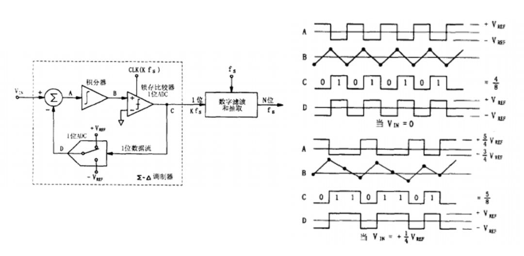
Figure 11 Outputs at Various Points of Σ-Δ ADC
Next, let’s look at the frequency domain characteristics of Σ-Δ. In Figure 12, U(S), N(S), and Y(S) represent the Laplace transforms of the input signal, quantization noise, and the filter input signal, respectively. The integrator acts as a filter in the frequency domain that is proportional to 1/s.When N(S) = 0, the relationship between Y(S) and U(S) is given by equation (1-5), indicating that the output and input have a transfer function of 1/s, which shows that the integrator exhibits low-pass filtering characteristics for the input signal. When U(S) = 0, the transfer function between the output and quantization noise is S/(1+S), indicating that for quantization noise, the Σ-Δ ADC exhibits high-pass filtering characteristics. These two formulas indicate that in Σ-Δ ADCs, quantization noise is no longer uniformly distributed across frequencies but is frequency-dependent and exhibits high-pass characteristics. This is the noise shaping technique of Σ-Δ. Through noise shaping, most of the energy of quantization noise is pushed to high frequencies, which will be filtered out by the subsequent low-pass filter, thus also helping to improve the SNR.
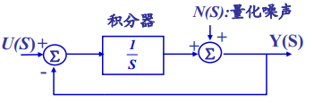
Figure 12 Frequency Domain Characteristics of Σ-Δ

Since noise shaping helps improve SNR, we certainly want its effect to be as great as possible. How can we enhance the effect of noise shaping? This can be achieved by increasing the order of the Σ-Δ. Figure 13 shows the structure of a second-order Σ-Δ ADC.In summary, we briefly introduced the three main techniques of Σ-Δ ADC: oversampling, noise shaping, and low-pass filtering. Figure 14 illustrates the relationship between oversampling ratio, order, and SNR. From the figure, it can be seen that the greater the oversampling ratio and the higher the order, the better the SNR.
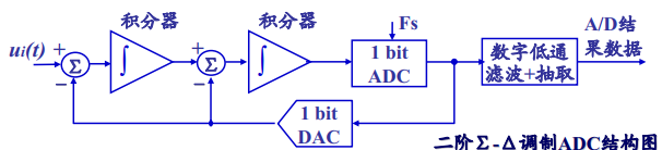
Figure 13 Structure of a Second-Order Σ-Δ ADC

Figure 14 Different Orders of Σ-Δ ADC