Welcome FPGA engineers to join the official WeChat technical group.
Clickthe blue textto follow us at FPGA Home – the largest pure FPGA engineer community in China.

1. Introduction
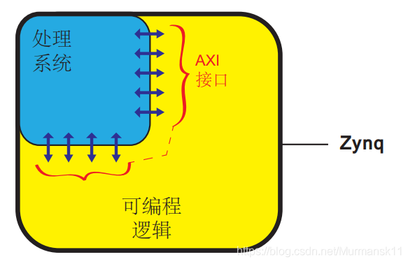
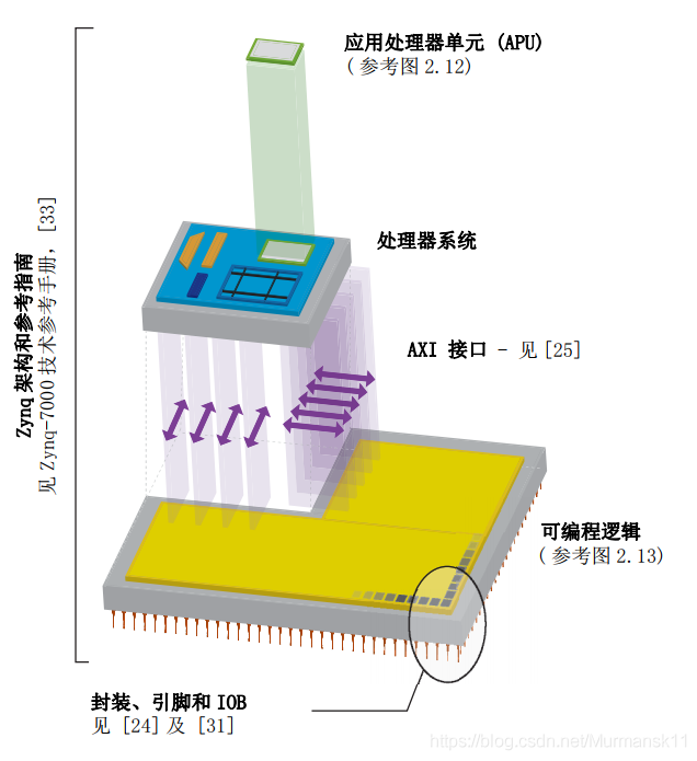
Zynq consists of two main parts: a processing system (PS) made up of dual-core ARM Cortex-A9 processors, and programmable logic (PL) equivalent to an FPGA. It also features integrated memory, various peripherals, and high-speed communication interfaces. This architecture implements the industrial standard AXI interface, providing high bandwidth and low latency connections between the two parts of the chip.
The PL part is ideal for implementing high-speed logic, arithmetic, and data stream subsystems, while the PS supports software programs or operating systems, with a fixed architecture that houses the processor and system memory. This means the entire functionality of any designed system can be appropriately divided between hardware and software. The link between PL and PS uses the industrial standard Advanced eXtensible Interface (AXI) connection method. These two parts can be used independently or together, and in fact, the power supply circuits are designed to independently power each part, allowing for power disconnection if either the PS or PL part is not in use.
2. Processor System (PS)
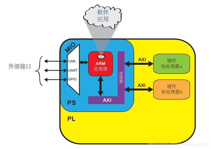
As the foundation of the processor system, all chips include a dual-core ARM Cortex-A9 processor. This is a “hard” processor – it is a dedicated and optimized silicon component on the chip. Xilinx’s MicroBlaze, a “soft” processor, is made up of units from the programmable logic part. This means that the implementation and deployment of a soft processor are equivalent to any other IP core in the FPGA’s logical structure. Generally, the advantage of a soft processor is the flexibility in the number of processor instances and precise implementations. On the other hand, hard processors can achieve relatively high performance, as is the case with Zynq’s ARM processor.
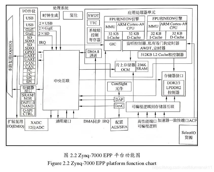
In Zynq’s processor system, there is not only the ARM processor but also a set of related processing resources, forming an Application Processing Unit (APU), along with extended peripheral interfaces, cache memory, memory interfaces, interconnect interfaces, and clock generation circuits. The following diagram shows the architecture block diagram of the PS part, with the highlighted part being the APU.
2.1 Application Processing Unit (APU)
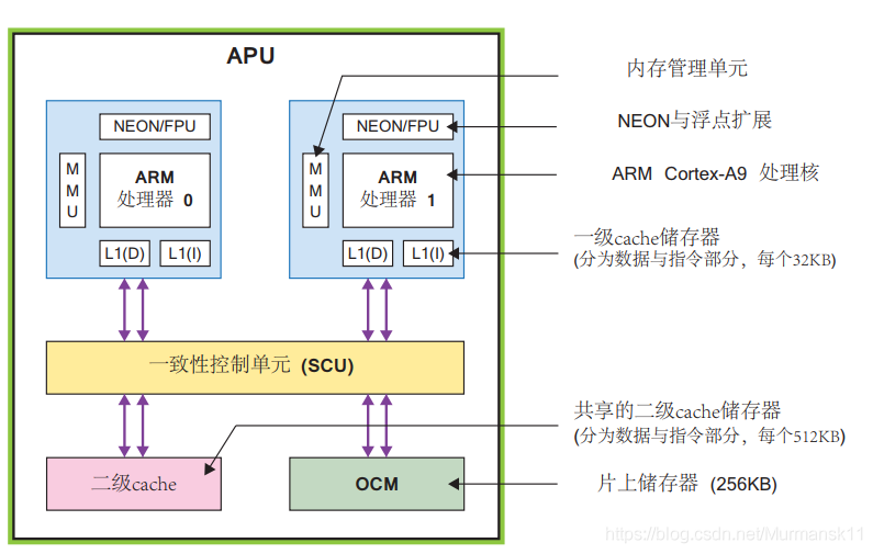
The APU mainly consists of two ARM processing cores with a maximum operating frequency of 1GHz;
A NEONTM media processing engine (Media Processing Engine, MPE) and a floating-point unit (Floating Point Unit, FPU);
A memory management unit (Memory Management Unit, MMU) that translates between virtual and physical addresses;
A level 1 cache memory (divided into instruction and data parts) with a level 2 cache memory; high-speed buffer between the CPU and memory;
On-chip memory (On Chip Memory, OCM);
A consistency control unit (Snoop Control Unit, SCU) that forms a bridge connection between ARM and the level 2 cache, OCM;
2.2 External Interfaces of the Processor System
Zynq PS implements numerous interfaces, both between PS and PL, and between PS and external components.
(1) Communication Between PS and External Interfaces
Communication between PS and external interfaces is mainly achieved through multiplexed input/output (Multiplexed Input/Output, MIO), which provides 54 pins that can be flexibly configured, indicating that the mapping between external devices and pins can be defined as needed.
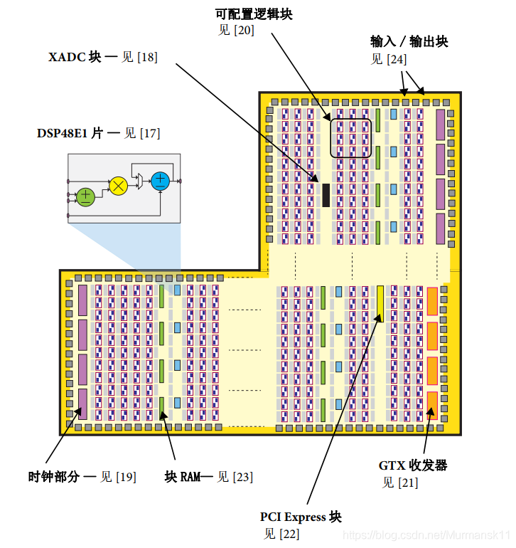
3. Programmable Logic (PL)
The second main part of the Zynq architecture is the programmable logic. This is based on Artix®-7 and Kintex®-7 FPGA components.
3.1 Logic Part
PL mainly consists of general-purpose FPGA logic, which is made up of logic slices (slice) and Configurable Logic Blocks (CLB), along with Input/Output Blocks (IOB) for interfaces.
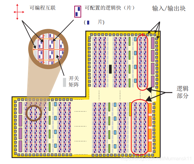
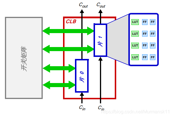
• Configurable Logic Block (CLB) — CLB is a small-scale, general grouping of logic units, arranged in a two-dimensional array in PL, connected via programmable interconnect to other similar resources. Each CLB contains two logic slices (slicem or slicel), and is adjacent to a switch matrix.
• Slice — A subunit within a CLB that contains resources for implementing combinational and sequential logic circuits. Zynq’s slices are composed of 4 lookup tables, 8 flip-flops, and other logic.
• Lookup Table (LUT) — A flexible resource that can implement: 1. Logic functions with up to 6 inputs; 2. A small read-only memory (ROM); 3. A small random-access memory (RAM); 4. A shift register. LUTs can be combined as needed to form larger logic functions, memory, or shift registers.
• Flip-flop (FF) — A sequential circuit that implements a 1-bit register with a reset function. One use of FF is to implement latches.
• Switch Matrix — Each CLB is adjacent to a switch matrix, providing flexible routing capabilities to connect 1. cells within the CLB; 2. a CLB to other resources in the PL.
• Carry Logic — Arithmetic circuits need to pass signals between adjacent slices, which is achieved through carry logic. Carry logic forms a chain of wiring and multiplexers to connect slices in a vertical column.
• Input/Output Blocks (IOB) — IOB implements the interfacing between PL logic resources and provides physical pads to connect to external circuits. Each IOB can handle one input or output signal. IOBs are typically located around the perimeter of the chip.
Although knowledge of the internal structure of the logic part is useful for designers, it is often not necessary to specifically designate these resources — Xilinx tools will automatically allocate the required LUTs, FFs, IOBs, etc., based on the design, and then perform the appropriate mapping. However, I still believe that having a clear understanding of the underlying circuit structure will greatly aid future learning.
3.2 Special Resources: DSP48E1 and Block RAM
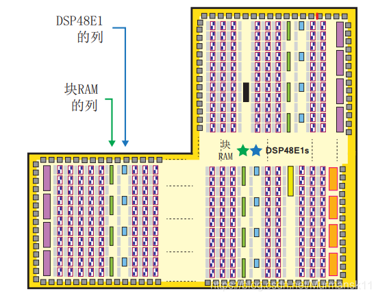
In addition to the general part, there are two special-purpose components: Block RAM for dense storage needs and DSP48E1 for high-speed arithmetic. These two resources are integrated in the logic array, arranged in columns, and are often located close to each other (since dense computation and data storage in memory are often closely related operations).
Each block RAM can store up to 36KB of information and can be configured as a 36KB RAM or two independent 18KB RAMs. The default word width is 18 bits, so each RAM contains 2048 storage units (2Kx18 bits). RAM can also be “reshaped” to contain more smaller units (for example, 4096 units x 9 bits, or 8192 x bits), or to form fewer longer units (such as 1024 units x 36 bits, 512 x 72 bits). Combining two or more block RAMs can create larger storage capacity. They can implement RAM, ROM, and FIFO buffers, and also support Error Correction Coding (ECC). Block RAM often operates at the highest clock frequency supported by the chip.
Distributed RAM, built using LUTs in the logic part. Implementing small storage with distributed RAM is often advantageous, both in terms of resource utilization and because this layout is more flexible (distributed storage can be placed near interacting components, allowing for faster timing performance).
(2) DSP48E1
The LUTs in the logic part can be used to implement arithmetic operations of any length, but they are most suitable for short word-length arithmetic operations (long word-length arithmetic circuits occupy considerable space in logic slices, and such layout and routing factors may lead to suboptimal clock frequencies).
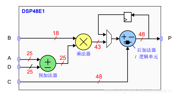
DSP48E1 is a logic slice specifically designed for high-speed arithmetic operations on long word-length signals. These are dedicated silicon resources, primarily containing pre-adders/subtractors, multipliers, and post-adders/subtractors within the logic unit.
4. Interface Between Processor System and Programmable Logic
The performance of Zynq relies not only on the characteristics of its two components, PS and PL, but also on the ability to integrate them into a complete, unified system. A key role in this is played by a set of highly customized AXI interconnects and interfaces that form a bridge between the two parts.
4.1 AXI Standard
AXI stands for Advanced eXtensible Interface. The AXI bus can be flexibly used and is generally employed to connect processors and other IP cores within an embedded system. In fact, there are three types of AXI4, each representing a different bus protocol, summarized below. The choice of which AXI bus protocol to use for a specific connection is based on the characteristics required for that connection.
• AXI4 — Used for memory-mapped connections, supporting the highest performance: data transfers of up to 256 data words (or “data beats”) for a given address.
• AXI4-Lite — A simplified connection that only supports transferring one data item (non-burst) per connection. AXI4-Lite is also memory-mapped: each transfer includes an address and a single data item.
• AXI4-Stream — Used for high-speed streaming data, supporting bulk transfers of data of unlimited size. There is no addressing mechanism, making this bus type most suitable for direct data flow between source and destination (non-memory mapped).
4.2 AXI Interconnect Interfaces
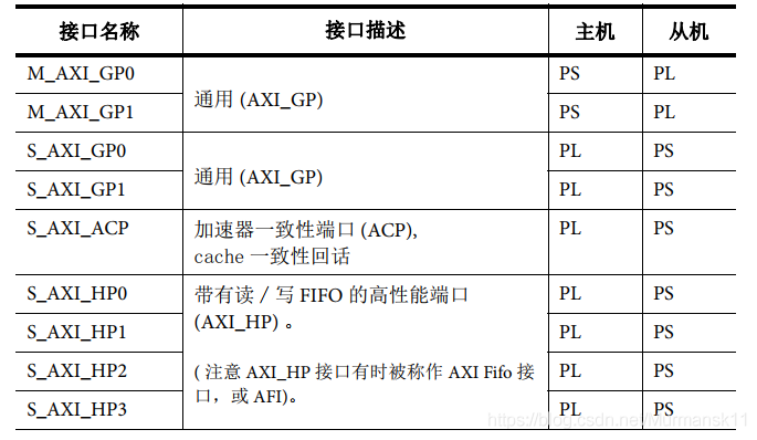
The main connection between PS and PL is through a set of 9 AXI interfaces, each comprising multiple channels. These form the internal interconnect within the PS and the connection to the PL.
• Interconnect — The interconnect is essentially a switch that manages and directly forwards communication between the connected AXI interfaces. There are several interconnects within the PS, some of which connect directly to the PL, while others are used only for internal connections. These interconnects are also formed using AXI interfaces.
• Interface — Point-to-point connections used to transmit data, addresses, and handshake signals between the host and slave within the system.
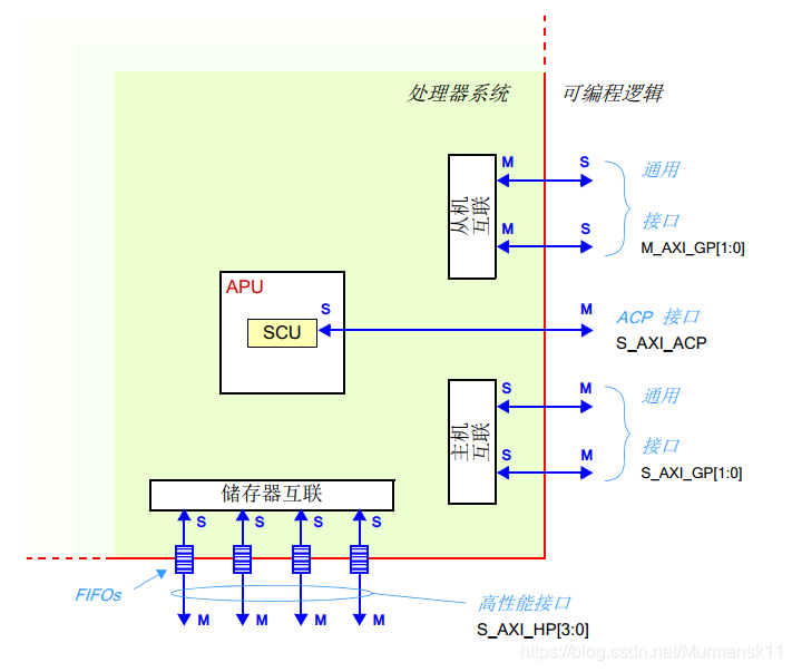
• General Purpose AXI — A 32-bit data bus suitable for medium to low-speed communication between PL and PS. The interface is pass-through without buffering. There are a total of four general-purpose interfaces: two PS masters and two PL masters. This interface can be enabled in the PS-PL Configuration for GP Master/Slave AXI Interface.
• Accelerator Coherency Port — A single asynchronous connection between the SCU in PL and APU, with a bus width of 64 bits. This port is used to achieve cache consistency between the APU and PL units. PL acts as the master. The ACP interface allows low-latency access to the PL master, with optional coherency and L1, L2 cache. From a system perspective, the ACP interface has connectivity similar to that of the APU CPU, allowing ACP to directly contend for resources in the APU block. This interface can be enabled in the PS-PL Configuration for ACP Slave AXI Interface.
• High-Performance Ports — Four high-performance AXI interfaces with FIFO buffers to provide “bulk” read/write operations, supporting high-rate communication between memory units in PL and PS. Data widths are 32 or 64 bits, with PL acting as the master in all four interfaces. The four AXI_HP interfaces provide high-bandwidth data channels to DDR and OCM memory for PL bus masters, with each interface having two FIFO buffers for read/write communication. The memory interconnect in PL routes the high-speed AXI_HP ports to two DDR memory ports or OCM. The AXI_HP interfaces can also be used as AXI_FIFO interfaces, leveraging their buffering capabilities. In short, this interface provides a high-throughput data channel between PL masters and PS memory (DDR or OCM). This can be enabled in the PS-PL Configuration for HP Slave AXI Interface.
This article is reprinted from:
https://blog.csdn.net/Murmansk11?type=blog
The content of this article represents the author’s views and does not represent the platform’s views.
If there are any objections, please feel free to contact us.

Scanto follow
FPGA Home

Welcome FPGA, embedded, signal processing engineers to follow our public account.
Attentionengineers!
We need you!

The largest FPGA technical community in the country

Welcome everyone to join the largest and strongest FPGA WeChat technical group, which has tens of thousands of engineers and a group of technology enthusiasts. Here, FPGA engineers help and share with each other, creating a strong technical atmosphere!Hurry up and invite your friends to join!

Press and hold to join the national FPGA technical group!

One of the best suppliers of Xilinx and Altera chips in the country!
Platform self-operated, import original quality guaranteed!
Continuously supplying multiple military research institutes and listed companies!
The best FPGA chip prices and the best after-sales service!
With the industry’s top service reputation!
Backed by the quality standards of top global suppliers!
Full series of XILINX orders or spot advantages!
XCVU9P-2FLGB2104I 200PCS
XCVU9P-2FLGA2104I 500PCS
XCVU13P-2FLGB2104I 300PCS
XC7K325T-2FFG900I 1500PCS
XC7K325T-2FFG676I 950PCS
XC7K160T-2FFG676I 850PCS
XC7VX690T-2FFG1927I Coming soon, please reserve!
XC7VX690T-2FFG1761I Coming soon, please reserve!
For more Xilinx model requests, please consult us! Thank you! Scan the QR code to join!

Official thanks to brands supporting the FPGA technical group: Xilinx, Intel (Altera), Microsemi (Actel), Lattice, Vantis, Quicklogic, Lucent, etc.!